The transistor is a ubiquitous and important component in modern microelectronics. Its purpose is simple: it allows you to manage a much stronger signal with a weak signal.
In particular, it can be used as a controlled "damper": by the absence of a signal on the "gate" to block the current flow, the supply is allowed. In other words: this is a button that is not pressed with a finger, but with a voltage supply. In digital electronics, this is the most common application.
Transistors are available in various enclosures: the same transistor can look quite different in different ways. In the prototyping more often than others there are cases:
TO-92 - compact, for small loads
TO-220AB - massive, well dissipating heat, for heavy loads
The designation on the schemes also varies depending on the type of transistor and the standard of designations used in the compilation. But regardless of the variation, its symbol remains recognizable.
Bipolar transistors
Bipolar transistors (BJT, Bipolar Junction Transistors) have three contacts:
Collector (collector) - it receives a high voltage, which you want to control
Base (base) - through it a small currentto unlock the big one; The base is grounded to block it
Emitter (emitter) - through it passes current from the collector and the base, when the transistor is "open"

The main characteristic of a bipolar transistor is the h fe also known as gain. It reflects how many times the larger current in the collector-emitter region is able to pass the transistor in relation to the base-emitter current.
For example, if h fe = 100, and 0.1 mA passes through the base, then the transistor will pass through itself as a maximum of 10 mA. If in this case there is a component on the high current section that consumes, for example, 8 mA, it will be provided with 8 mA, and the transistor will have a "reserve". If there is a component that consumes 20 mA, only the maximum 10 mA will be provided to it.
Also, the documentation for each transistor indicates the maximum permissible voltages and currents on the contacts. Exceeding these values leads to excessive heating and reduced service, and a strong excess can lead to destruction.
NPN and PNP
The transistor described above is a so-called NPN transistor. It is called so because it consists of three layers of silicon, connected in the order: Negative-Positive-Negative. Where negative is a silicon alloy possessing an excess of negative charge carriers (n-doped), and positive - with an excess of positive (p-doped).
NPNs are more effective and common in the industry.
PNP-transistors in the designation differ in the direction of the arrow. The arrow always points from P to N. PNP transistors differ in "inverted" behavior: the current is not blocked when the base is grounded and blocked when current flows through it.
Field Effect Transistors
Field effect transistors (FET, Field Effect Transistor) have the same function, but differ internally. A particular type of these components are the MOSFET (Metal-Oxide-Semiconductor Field Effect Transistor) transistors. They allow us to operate with much larger capacities at the same size. And the control of the "damper" itself is carried out exclusively with the help of tension: the current through the gate, unlike bipolar transistors, does not go.
Field-effect transistors have three contacts:
Stoke (drain) - it is supplied with a high voltage, which you want to control
Gate (gate) - voltage is applied to it to allow current flow; The gate is grounded to block the current.
Source - through it passes current from the drain, when the transistor is "open"

N-Channel and P-Channel

By analogy with bipolar transistors, the field is distinguished by polarity. Above was described the N-channel transistor. They are most common.
P-Channel in the designation differs in the direction of the arrow and, again, has an "inverted" behavior.
Connecting transistors to control powerful components
A typical task of the microcontroller is to enable and disable a specific component of the circuit. The microcontroller itself usually has modest characteristics with respect to the power withstand. So Arduino, with a 5 V output, can withstand a current of 40 mA. Powerful motors or super-bright LEDs can consume hundreds of milliamperes. When connecting such loads directly, the chip can quickly fail. In addition, some components require more than 5 V for operation, and Arduino can not issue a digital output pin (more than 5 V) from the output pin.
But, it is easy enough to control a transistor, which in turn will control a large current. Let's say we need to connect a long LED strip that requires 12 V and at the same time consumes 100 mA:

Now when setting the output to the logical unit (high), the input to the 5 V base will open the transistor and the current will flow through the tape - it will glow. When the output is set to logic zero (low), the base will be grounded through the microcontroller, and the current flow is blocked.
pay attention to current limiting resistor R. It is necessary that when the control voltage is applied, there is no short circuit along the route microcontroller-transistor-earth. The main thing is not to exceed the permissible current through the Arduino contact in 40 mA, so you need to use a resistor of at least:
here U d is the voltage drop across the transistor itself. It depends on the material of which it is made and is usually 0.3 - 0.6 V.
But it is not necessary to keep the current at the limit of permissible. It is only necessary that the gain of the transistor allows controlling the necessary current. In our case it is 100 mA. Suppose for the used transistor h fe = 100, then we will have enough control current in 1 mA
We will use a resistor rated at 118 ohms to 4.7 kilohms. For stable operation on one side and a small load on the chip on the other, 2.2 kOhm is a good choice.
If you use a field bipolar transistor, you can do without a resistor:
![]()
this is due to the fact that the gate in such transistors is controlled exclusively by voltage: the current on the microcontroller - gate - source is absent. And thanks to its high performance, the scheme using MOSFET allows you to manage very powerful components.
The necessary explanations are given, we go to the point.
Transistors. Definition and history
Transistor - an electronic semiconductor device in which the current in the circuit of the two electrodes is controlled by a third electrode. (tranzistors.ru)
The first were invented field-effect transistors (1928), and bipolar appeared in 1947 in the laboratory of Bell Labs. And it was, without exaggeration, a revolution in electronics.
Very quickly transistors replaced vacuum lamps in various electronic devices. In connection with this, the reliability of such devices has increased and their dimensions have considerably diminished. And to this day, no matter how "heaped" was not the chip, it still contains a lot of transistors (as well as diodes, capacitors, resistors, etc.). Only very small.
By the way, initially "transistors" were called resistors whose resistance could be changed by means of the applied voltage. If we ignore the physics of processes, then a modern transistor can also be represented as a resistance, depending on the signal applied to it.
What is the difference between field and bipolar transistors? The answer lies in the names themselves. In a bipolar transistor, charge transfer involves and electrons, and hole ("encore" - twice). And in the field (it's unipolar) - or electrons, or holes.
Also, these types of transistors vary in their applications. Bipolar ones are used mainly in analog technology, and field ones - in digital.
And, at last: the main field of application of any transistors - amplification of a weak signal due to an additional power source.
Bipolar transistor. Principle of operation. Main characteristics

The bipolar transistor consists of three regions: an emitter, a base and a collector, each of which is energized. Depending on the type of conductivity of these regions, n-p-n and p-n-p transistors are isolated. Usually the collector area is wider than the emitter. The base is made of a low-alloy semiconductor (because of which it has a large resistance) and is made very thin. Since the contact area of the emitter-base is much less than the base-to-collector contact area, it is not possible to change the emitter and collector locally by changing the polarity of the connection. Thus, the transistor refers to unbalanced devices.
Before considering the physics of the transistor, we will outline the general problem. 
It consists of the following: a strong current flows between the emitter and the collector ( collector current), and between the emitter and the base is a weak control current ( base current). The collector current will vary depending on the change in the base current. Why?
Consider the p-n transitions of the transistor. There are two of them: the emitter-base (EB) and the base-collector (BC). In the active mode of the transistor, the first one is connected to the direct one, and the second one is connected to the reverse bias. What happens in the p-n junctions? For greater certainty, we will consider an n-p-n transistor. For p-n-p all is analogous, only the word "electrons" needs to be replaced with "holes".
Since the ED transition is open, then the electrons easily "run over" to the base. There they partially recombine with holes, but aboutmost of them because of the small thickness of the base and its weak doping can reach the base-collector transition. Which, as we recall, is included with a reverse bias. And since in the base electrons are minority charge carriers, the elec- tric transition field helps them overcome it. Thus, the collector current is only slightly less than the emitter current. Now watch your hands. If we increase the base current, then the EB transition will open more strongly, and more electrons can cross the emitter and collector. And since the collector current is initially greater than the base current, this change will be very, very noticeable. In this way, there will be an amplification of a weak signal arriving at the base. Once again: a strong change in the collector current is a proportional reflection of a weak change in the base current.
I remember my teammates explain the principle of bipolar transistor operation using the example of a water tap. The water in it is the collector current, and the control current of the base is how much we rotate the handle. A small amount of effort (control action) is necessary to increase the flow of water from the tap.
In addition to the processes discussed, a number of phenomena can occur at the p-n junctions of the transistor. For example, with a strong voltage increase at the base-collector transition, avalanche charge multiplication may occur due to impact ionization. Together with the tunneling effect, this will first give an electric effect, and then (with increasing current) and thermal breakdown. However, a thermal breakdown in a transistor can occur without an electrical (that is, without increasing the collector voltage to the breakdown voltage). For this, one excessive current through the collector will suffice.
Another phenomenon is related to the fact that when the stresses change on the collector and emitter junctions, their thickness changes. And if the base is too thin, then the closing effect (the so-called "puncture" of the base) can occur-the junction of the collector junction with the emitter one. In this case, the base area disappears, and the transistor stops working normally.
The collector current of the transistor in the normal active mode of operation of the transistor is greater than the base current a certain number of times. This number is called current amplification factor and is one of the main parameters of the transistor. It is denoted by h21. If the transistor is switched on without load on the collector, then at a constant collector-emitter voltage, the ratio of the collector current to the base current will give static current gain. It can be equal to tens or hundreds of units, but it is worth taking into account the fact that in real schemes this coefficient is less due to the fact that when the load is switched on the collector current decreases regularly.
The second important parameter is input resistance of the transistor. According to Ohm's law, it is the ratio of the voltage between the base and the emitter to the current control base. The larger it is, the lower the base current and the higher the gain.
The third parameter of the bipolar transistor - voltage gain. It is equal to the ratio of the amplitude or effective values of the output (emitter-collector) and input (base-emitter) variable voltages. Since the first value is usually very large (units and tens of volts), and the second is very small (tenths of a volt), this coefficient can reach tens of thousands of units. It should be noted that each control signal of the base has its own voltage gain.
Also transistors have frequency response, which characterizes the ability of the transistor to amplify a signal whose frequency approaches the boundary frequency of amplification. The point is that with increasing frequency of the input signal the gain is reduced. This is due to the fact that the time of the flow of the basic physical processes (the time of carrier transfer from the emitter to the collector, the charge and discharge of barrier capacitive transitions) becomes commensurable with the period of the change in the input signal. Those. the transistor simply does not have time to respond to changes in the input signal and at some point just stops amplifying it. The frequency at which this occurs is called the boundary.
Also the parameters of the bipolar transistor are:
- collector-emitter return current
- on time
- back current of the collector
- maximum permissible current
The conventions for n-p-n and p-n-p transistors differ only in the direction of the arrow indicating the emitter. It shows how the current flows in this transistor.
Operating modes of bipolar transistor
The above option is a normal active mode of operation of the transistor. However, there are several more open / closed combinations of p-n junctions, each of which represents a separate mode of operation of the transistor.- Inverse active mode. Here the transition of the BC is open, and the EB is closed on the contrary. Strengthening properties in this mode, of course, is nowhere worse, therefore transistors in this mode are used very rarely.
- Saturation mode. Both transitions are open. Accordingly, the main charge carriers of the collector and the emitter "run" to the base, where they actively recombine with its main carriers. Because of the emerging redundancy of the charge carriers, the resistance of the base and p-n junctions decreases. Therefore, a circuit containing a transistor in saturation mode can be considered short-circuited, and the radio element itself can be represented as an equipotential point.
- Cutoff mode. Both transitions of the transistor are closed, i.e. the current of the main charge carriers between the emitter and the collector stops. Streams of minority charge carriers create only small and uncontrolled thermal currents of transitions. Because of the poverty of the base and the transitions of charge carriers, their resistance greatly increases. Therefore, it is often believed that a transistor operating in the cut-off mode is a circuit break.
- Barrier mode In this mode, the base is directly or through a low resistance closed to the collector. Also in the collector or emitter circuit include a resistor, which sets the current through the transistor. Thus, the equivalent circuit of a diode with a series-connected resistance is obtained. This mode is very useful, since it allows the circuit to work at almost any frequency, over a wide temperature range and is undemanding to the parameters of transistors.
Bipolar transistor switching circuits
Since there are three contacts for the transistor, in the general case, it must be fed from two sources, which together produce four outputs. Therefore, one of the contacts of the transistor has to supply the voltage of the same sign from both sources. And, depending on what kind of contact this is, three circuits for switching on bipolar transistors are distinguished: with a common emitter (OE), a common collector (OK), and a common base (OB). Each of them has both advantages and disadvantages. The choice between them is done depending on what parameters are important to us, and what can be sacrificed.
The circuit with a common emitter

This circuit gives the greatest gain in voltage and current (and hence the power - up to tens of thousands of units), in connection with which is the most common. Here, the emitter-base transition is switched directly, and the base-collector transition is reversed. And since both the base and the collector are supplied with a voltage of the same sign, the circuit can be fed from a single source. In this scheme, the phase of the output AC voltage varies with respect to the phase of the input AC voltage by 180 degrees.
But to all buns, the scheme with the MA has a significant drawback. It consists in the fact that the increase in frequency and temperature leads to a significant deterioration of the amplifying properties of the transistor. Thus, if the transistor is to operate at high frequencies, it is better to use a different switching circuit. For example, with a common base.
Scheme of inclusion with a common base

This circuit does not provide significant signal amplification, but it is good at high frequencies, since it allows fuller use of the frequency characteristic of the transistor. If the same transistor is switched on first with a common emitter and then with a common base, then in the second case there will be a significant increase in its limiting gain frequency. Since with this connection the input resistance is low and the output resistance is not very high, then the cascades of transistors assembled according to the scheme with OB are used in antenna amplifiers, where the cable impedance usually does not exceed 100 ohms.
In a circuit with a common base, the phase of the signal is not inverted, and the noise level at high frequencies is reduced. But, as already mentioned, the current gain factor is always slightly less than unity. True, the voltage gain is the same here as in the common-emitter circuit. To drawbacks of the scheme with a common base can also be attributed the need to use two power sources.
Scheme of inclusion with a common collector

The peculiarity of this scheme is that the input voltage is completely transmitted back to the input, that is, the negative feedback is very strong.
I recall that negative feedback is called such that the output signal is fed back to the input, which reduces the level of the input signal. Thus, there is an automatic correction with random variation of the input signal parameters
The current gain is almost the same as in the common-emitter circuit. But the voltage gain is small (the main drawback of this scheme). It approaches unity, but is always less than unity. Thus, the power gain factor is only a few dozen units.
In a circuit with a common collector, there is no phase shift between the input and output voltages. Since the voltage gain is close to unity, the output voltage in phase and amplitude coincides with the input voltage, ie repeats it. That is why such a scheme is called an emitter follower. Emitter - because the output voltage is removed from the emitter relative to the common wire.
This switching is used to match the transistor stages or when the input source has a high input resistance (for example, a piezoelectric pickup or a condenser microphone).
Two words about cascades
It happens that you need to increase the output power (ie increase the collector current). In this case, the parallel inclusion of the required number of transistors is used.
Naturally, they should be approximately the same in terms of characteristics. But it must be remembered that the maximum total collector current should not exceed 1.6-1.7 of the maximum collector current of any of the cascade transistors.
Nevertheless (thanks for the remark), in the case of bipolar transistors, this is not recommended. Because two transistors even one typo at least a little, but differ from each other. Accordingly, with parallel inclusion, currents of different sizes will flow through them. To balance these currents in the emitter circuits of the transistors, balance resistors are put. The magnitude of their resistance is calculated so that the voltage drop across them in the working current range is not less than 0.7 V. It is clear that this leads to a significant deterioration in the efficiency of the circuit.
There may also be a need for a transistor with good sensitivity and at the same time with a good gain. In such cases, a cascade of a sensitive but low-power transistor is used (in the figure - VT1), which controls the energy supply of a more powerful colleague (in the figure - VT2). 
Other applications of bipolar transistors
Transistors can be used not only for signal amplification circuits. For example, due to the fact that they can operate in saturation and cutoff modes, they are used as electronic keys. It is also possible to use transistors in signal generator circuits. If they work in the key mode, then a rectangular signal will be generated, and if in the amplification mode - then the signal is arbitrary shape, depending on the control action.Marking
Since the article has already grown to an indecently large amount, at this point I will simply give two good references on which the basic systems of marking semiconductor devices (including transistors) are described in detail: http://kazus.ru/guide/transistors/mark_all.html and file.xls (35 kb).Useful comments:
http://habrahabr.ru/blogs/easyelectronics/133136/#comment_4419173
Tags: Add Tags
The device and the principle of operation
The first transistors were made on the basis of germany . At present, they are made mainly from silicon and gallium arsenide . The latest transistors are used in high-frequency amplifier circuits. The bipolar transistor consists of three different ways alloyed semiconductor zones: emitter E, the base B and collector C. Depending on the type of conductivity of these zones, NPN (emitter-n-semiconductor, base-p-semiconductor, collector-n-semiconductor) and PNP transistors are distinguished. Conductive contacts are connected to each of the zones. The base is located between the emitter and the collector and is made of a weakly doped semiconductor with a high resistance. The total area of the base-emitter contact is much less than the collector-base contact area (this is done for two reasons: a large collector-base junction area increases the probability of extraction of minority charge carriers into the collector and since in the operating mode the collector- offset, which increases heat generation, contributes to heat removal from the collector), so a general bipolar transistor is an asymmetric device (it is impossible by reversing the polarity of the connection to swap places and the emitter and collector and get as a result an absolutely similar to the original bipolar transistor).
In the active mode of operation, the transistor is turned on so that its emitter junction biased in the forward direction (open), and the collector transition is biased in the opposite direction (closed). For definiteness, let us consider npn transistor, all the arguments are repeated in exactly the same way for the case pnp transistor, with the replacement of the word "electrons" with "holes", and vice versa, and with the replacement of all voltages by opposite signs. AT npn transistor, electrons, the main current carriers in the emitter, pass through the open emitter-base junction injected) to the base area. A part of these electrons recombines with the main charge carriers in the base (holes). However, because the base is made very thin and relatively lightly doped, most of the electrons injected from the emitter diffuse into the collector region. A strong electric field of a backwardly biased collector junction captures electrons, and carries them to the collector. The collector current is thus almost equal to the current of the emitter, with the exception of a small loss of recombination in the base, which forms the base current (I e = I b + I k). The coefficient α, which connects the emitter current and the collector current (I k = α I 1 Oe) is called the current transfer coefficient of the emitter. The numerical value of the coefficient α 0.9 is 0.999. The higher the ratio, the more efficient the transistor transmits current. This coefficient depends little on the collector-base and base-emitter voltages. Therefore, over a wide range of operating voltages, the collector current is proportional to the base current, the proportionality factor is β = α / (1 - α) = (10..1000). Thus, by changing the low current of the base, it is possible to control a much larger collector current.
Operating modes of bipolar transistor
Normal active mode
The emitter-base transition is switched on in the forward direction (open), and the collector-base junction is in the reverse (closed)
U E\u003e 0; U KB<0 (для транзистора p-n-p типа, для транзистора n-p-n типа условие будет иметь вид U ЭБ <0;U КБ >0);
Inverse active mode
The emitter junction has a reverse inclusion, and the collector junction is direct.
Saturation mode
Both p-n junctions are biased in the forward direction (both are open). If the emitter and collector pn junctions are connected to external sources in the forward direction, the transistor will be in saturation mode. The diffusion electric field of the emitter and collector transitions will be partially attenuated by the electric field created by the external sources UeB and UKB. As a result, the potential barrier limiting the diffusion of the main charge carriers will decrease, and the penetration (injection) of holes from the emitter and collector into the base will begin, that is, currents called saturation currents of the emitter (IE.nas) and collector (IK) will flow through the emitter and collector of the transistor. us).
Cutoff mode
In this mode, both p-n junctions of the device are offset in the opposite direction (both are closed). The cut-off mode of the transistor is obtained when the emitter and collector pn junctions are connected to external sources in the opposite direction. In this case, very small reverse currents of the emitter (IBO) and the collector (IKBO) flow through both pn-junctions. The current of the base is equal to the sum of these currents and, depending on the type of transistor, ranges from microampere-μA units (for silicon transistors) to milliampere-mA units (for germanium transistors).
Barrier mode
In this mode base the transistor on a direct current is connected shortly or through a small resistor with its collector, while in collector or in emitter the transistor circuit turns on a resistor that sets the current through the transistor. In this connection, the transistor is a kind of diode, connected in series with the current-setting resistor. Such schemes of cascades are characterized by a small number of components, a good high-frequency decoupling, a large operating temperature range, insensitivity to the parameters of transistors.
Schemes of inclusion
Any circuit incorporating a transistor is characterized by two main indicators:
- Current gain I IO / I IN.
- Input resistance R in = U in / I in
Scheme of inclusion with a common base
Amplifier with a common base.
- Among all three configurations, it has the smallest input and largest output resistance. Has a current gain close to unity, and a large voltage gain. The phase of the signal is not inverted.
- Current gain: I out / I in = I к / I э = α [α<1]
- The input resistance R in = Uin / Iin = U be / Ie.
The input impedance for a circuit with a common base is small and does not exceed 100 Ω for low-power transistors, since the input circuit of the transistor is thus an open emitter junction of the transistor.
Pluses:
- Good temperature and frequency properties.
- High allowable voltage
Disadvantages of the scheme with a common base:
- Low current gain, since α< 1
- Low input resistance
- Two different voltage sources for power supply.
The circuit with a common emitter
- Current gain: I out / I in = I k / I b = I k / (I e -I k) = α / (1-α) = β [β \u003e\u003e 1]
- Input resistance: R in = U in / I in = U be / I b
Pluses:
- High current gain
- High voltage gain
- The greatest gain in power
- You can do with one power source
- The output AC voltage is inverted with respect to the input voltage.
Disadvantages:
- The worst temperature and frequency characteristics in comparison with the scheme with a common base
The scheme with a common collector
- Current gain factor: I out / I in = Ie / I b = I e / (I e -I k) = 1 / (1-α) = β [β \u003e\u003e 1]
- Input resistance: R in = U in / I in = (U be + U kOe) / I b
Pluses:
- Large input resistance
- Low output resistance
Disadvantages:
- The voltage gain is less than 1.
A circuit with such an inclusion is called an "emitter follower"
Main settings
- Current transmission ratio
- Input impedance
- Output conductivity
- Collector-emitter return current
- Switch-on time
- The limiting frequency of the base current transfer coefficient
- Reverse Collector Current
- Maximum allowable current
- Boundary frequency of the current transfer coefficient in a common-emitter circuit
The parameters of the transistor are divided into their own (primary) and secondary. Own parameters characterize the properties of the transistor, regardless of the scheme of its inclusion. The following are assumed as the main parameters:
- current gain α;
- resistance of the emitter, collector and base to the alternating current r e, r k, r b, which are:
- r e is the sum of the resistances of the emitter region and the emitter junction;
- r k is the sum of the resistances of the collector region and the collector junction;
- r b is the transverse resistance of the base.
Equivalent circuit of a bipolar transistor with the use of h-parameters
Secondary parameters are different for different switching circuits of the transistor and, due to its nonlinearity, are valid only for low frequencies and small signal amplitudes. For secondary parameters, several systems of parameters and corresponding equivalent schemes are proposed. The main ones are mixed (hybrid) parameters, denoted by the letter "h".
Input impedance - resistance of the transistor to the input alternating current with a short circuit at the output. The change in the input current is the result of a change in the input voltage, without the influence of feedback on the output voltage.
H 11 = U m1 / I m1 for U m2 = 0.
Voltage feedback ratio shows how much of the output AC voltage is transferred to the input of the transistor due to feedback in it. In the input circuit of the transistor there is no alternating current, and the change in the input voltage occurs only as a result of a change in the output voltage.
H 12 = U m1 / U m2 for I m1 = 0.
Current transmission ratio (current gain) shows the AC gain at zero load resistance. The output current depends only on the input current without affecting the output voltage.
H 21 = I m2 / I m1 for U m2 = 0.
Output conductivity - Internal conductivity for alternating current between output terminals. The output current varies with the output voltage.
H 22 = I m2 / U m2 for I m1 = 0.
The relationship between alternating currents and transistor voltages is expressed by the equations:
U m1 = h 11 I m1 + h 12 U m2;
I m2 = h 21 I m1 + h 22 U m2.
Depending on the switching circuit of the transistor, the letters h are added to the digital indices of the h-parameters: "e" - for the OE scheme, "b" for the OB scheme, "k" for the OK scheme.
For the OE scheme: I m1 = I mb, I m2 = I mk, U m1 = U mb-e, U m2 = U mk-e. For example, for this scheme:
H 21e = I mk / I mb = β.
For the OB scheme: I m1 = I m, I m2 = I mk, U m1 = U m-b, U m2 = U mk-b.
The intrinsic parameters of the transistor are related to the h-parameters, for example for the OE circuit:
| ; | ; | ; | . |
With increasing frequency, the capacitance of the collector junction C k begins to exert a deleterious effect on the operation of the transistor. The capacitance resistance decreases, the current through the load resistance decreases and, consequently, the gain factors α and β. The resistance of the capacitance of the emitter junction C e also decreases, but it is shunted by a small resistance of the transition r e and in most cases can be ignored. In addition, as the frequency increases, the coefficient β is further reduced as a result of the delay in the phase of the collector current from the phase of the emitter current, which is caused by the inertness of the transport of carriers through the base from the emitter to the collector and inertial processes of accumulation and charge dissipation in the base. The frequencies at which the α and β coefficients decrease by 3 dB are called boundary frequencies of the current transfer coefficient for the OB and OE schemes, respectively.
In pulse mode, the collector current pulse starts with a delay of the delay time τ 3 with respect to the input current pulse, which is caused by the finite carrier travel time through the base. As the carriers accumulate in the base, the collector current rises during the duration of the front τ φ. Turn-on time The transistor is called τ on = τ 3 + τ φ.
The designation of bipolar transistors on circuits
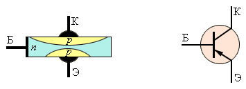
Bipolar transistor - three-electrode semiconductor device , one of the types transistors . In the semiconductor structure, 2 p-n junctions and transfer charge in the device is carried by carriers of 2 kinds - electrons and holes . That is why the device was called "bipolar".
It is used in electronic devices to amplify the generation of electrical oscillations and as a switching current element, for example, in logical electronic circuits.
The electrodes are connected to three successive layers of a semiconductor with an alternating type impurity conduction . By this method, alternations are distinguished n-p-n and p-n-p transistors ( n (negative) is the electronic type of impurity conduction, p (positive) is a hole one).
The operation of a bipolar transistor, in contrast to fET , is based on the transfer charges at the same time of two types, carriers of which are electrons and holes (from the word "bi" to "two"). The schematic device of the transistor is shown in the second figure.
The electrode connected to the middle layer is called base, the electrodes connected to the outer layers are called emitter and collector. From the point of view of the types of conductivity, the emitter and collector layers are not distinguishable. But in practice, in the manufacture of transistors, to improve the electrical parameters of the device, they differ significantly in the degree of doping with impurities. The emitter layer is heavily doped, the collector layer is weakly doped, which provides an increase in the allowable collector voltage. The magnitude of the breakdown reverse voltage of the emitter junction is not critical, since usually in electronic circuits the transistors work with a direct-shifted emitter p-n-junction , in addition, strong doping of the emitter layer provides a better injection non-basic carriers in the base layer, which increases the current transmission ratio in circuits with a common base. In addition, the area of the collector p-n-junction In manufacturing, much more emitter junction area is made, which ensures better collection of minority carriers from the base layer and improves the transmission coefficient.
To increase the speed (frequency parameters) of a bipolar transistor, the thickness of the base layer must be made thinner, since the thickness of the base layer, including the time of "span" (diffusion in the non-drift devices) of minority carriers, but, with a decrease in the thickness of the base, the limiting collector voltage, so the thickness of the base layer is chosen based on a reasonable compromise.
The device and the principle of operation
In the first transistors as a semiconductor material was used metallic germanium . In the present (2015) time they are made mainly from single-crystal silicon and single-crystal gallium arsenide . Due to the very high mobility of carriers in gallium arsenide, devices based on it are of high speed and are used in superfast logical schemes and in the schemes Microwave -amplifiers.
The bipolar transistor consists of three different ways alloyed semiconductor layers: emitter E (E), the base B (B) and collector C (TO). Depending on the alternation of the conductivity type of these layers, n-p-n (emitter - n-semiconductor, base - psemiconductor, collector - n-semiconductor) and p-n-p transistors. Conductive non-directional contacts are connected to each of the layers.
The base layer is located between the emitter and collector layers and is slightly doped, therefore it has a large electrical resistance . The total area of the base-emitter contact is much less than the collector-base contact area (this is done for two reasons: a large collector-base junction area increases the probability of capturing minority carriers from the base to the collector and, since in operation, the collector- with reverse bias, when working in the collector transition, the main part of the heat dissipated by the device is allocated, increasing the area contributes to better heat removal from the collector junction), so the real bipolar a general-purpose transistor is an asymmetric device (it is technically inappropriate to swap the emitter and collector and obtain a similar bipolar transistor-inverse inclusion).
In the active amplification mode of operation, the transistor is switched on so that its emitter junction biased in the forward direction (open), and the collector transition is biased in the opposite direction (closed).
For definiteness, let us consider the work n-p-n transistor, all the arguments are repeated in exactly the same way for the case p-n-p transistor, with the replacement of the word "electrons" with "holes", and vice versa, and with the replacement of all voltages by opposite signs. AT n-p-n transistor electrons, the main charge carriers in the emitter, pass through the open emitter-base junction ( injected) to the base area. A part of these electrons recombines with the main charge carriers in the base (holes). However, because the base is made very thin and relatively lightly doped, most of the electrons injected from the emitter diffuse into the collector region, since the recombination time is relatively large. A strong electric field of a reverse biased collector junction captures the minority carriers from the base (electrons), and transfers them to the collector layer. The collector current is thus almost equal to the current of the emitter, except for a small loss of recombination in the base, which forms the base current ( I e = I b + I k).
The coefficient α, which connects the emitter current and the collector current ( I к = α I э э) is called emitter current transfer factor. The numerical value of the coefficient is α 0,9-0,999. The higher the ratio, the more efficient the transistor transmits current. This coefficient depends little on the collector-base and base-emitter voltages. Therefore, over a wide range of operating voltages, the collector current is proportional to the base current, the proportionality factor is β = α / (1 - α), from 10 to 1000. Thus, a much higher current of the reservoir can be controlled by a small current of the base.
Operating modes of bipolar transistor
| Stresses on the emitter, base, collector () |
Bias transition base-emitter for the type n-p-n |
Bias transition base collector for the type n-p-n |
Mode for the type n-p-n |
|---|---|---|---|
| direct | the reverse | normal active mode |
|
| direct | direct | saturation mode | |
| the reverse | the reverse | cutoff mode | |
| the reverse | direct | inverted active mode |
|
| Stresses on the emitter, base, collector () |
Bias transition base-emitter for the type p-n-p |
Bias transition base collector for the type p-n-p |
Mode for the type p-n-p |
| the reverse | direct | inverted active mode |
|
| the reverse | the reverse | cutoff mode | |
| direct | direct | saturation mode | |
| direct | the reverse | normal active mode |
Normal active mode
The emitter-base transition is switched on in the forward direction (open), and the collector-base junction is in the reverse direction (closed):
U E\u003e0; U KB< 0 (for the transistor n-p-n type), for the transistor p-n-p type condition will have the form U EB<0; U KB\u003e0.Inverse active mode
The emitter junction has a reverse bias, and the collector junction is direct: U KB\u003e0; U EB< 0 (for the transistor n-p-n type).
Saturation mode
Both p-n Transitions are biased in the forward direction (both are open). If the emitter and collector pn-transfers to connect to external sources in the forward direction, the transistor will be in saturation mode. The diffusion electric field of the emitter and collector junctions will be partially attenuated by an electric field created by external sources Web and UCB. As a result, the potential barrier limiting the diffusion of the main charge carriers will decrease and the penetration (injection) of holes from the emitter and collector into the base will begin, that is, currents called saturation currents of the emitter will flow through the emitter and collector of the transistor I E. Us) and the collector ( I K. us).
Collector-emitter saturation voltage (U КЭ. Us) is a voltage drop on an open transistor (the semantic analogue R SI. ot in field effect transistors). Similarly base-emitter saturation voltage (U BE) is the voltage drop between the base and the emitter on an open transistor.
Cutoff mode
In this mode, both p-n transition are displaced in the opposite direction. The cut-off condition corresponds to condition U EB<0, U KB<0.
Barrier mode
In this mode base the transistor on a direct current is connected shortly or through a small resistor with its collector, while in collector or in emitter the transistor circuit turns on a resistor that sets the current through the transistor. In this connection, the transistor is a kind of diode, connected in series with the current-setting resistor. Such schemes of cascades are characterized by a small number of components, a good high-frequency decoupling, a large operating temperature range, insensitivity to the parameters of transistors.
Schemes of inclusion
Any circuit incorporating a transistor is characterized by two main indicators:
- Current gain I out / I in.
- Input impedance R in = U in / I in.
Scheme of inclusion with a common base

Scheme of inclusion with a common base.
Amplifier with a common base.
- Among all three configurations, it has the smallest input and largest output resistance. Has a current gain close to unity, and a large voltage gain. Does not invert the phase of the signal.
- I out / I in = I to / I e = α [α<1].
- Input impedance R in = U in / I in = U eb / I e.
Input resistance (input impedance) of the amplification stage with a common base is small, depends on the emitter current, when the current is increased, it decreases and does not exceed unity-hundreds of ohms for low-power cascades, since the input circuit of the cascade is an open emitter junction of the transistor.
Advantages
- Good temperature and wide frequency range, as in this scheme is suppressed miller effect.
- High permissible collector voltage.
- A small current gain of α, since α is always slightly less than 1
- Low input resistance
The circuit with a common emitter

A circuit with a common emitter.
I out = I to
I in = I b
U in = U be
U out = U koe.
- Current gain: I out / I in = I to / I b = I to / ( I e -I k) = α / (1-α) = β [β \u003e\u003e 1].
- Input impedance: R in = U in / I in = U be / I b.
- High current gain.
- High voltage gain.
- The greatest gain in power.
- You can do with one power source.
- The output AC voltage is inverted with respect to the input voltage.
- Has a lower temperature stability. The frequency properties of this inclusion in comparison with the scheme with a common base are significantly worse, which is due to effect of Miller.
The scheme with a common collector

Scheme of inclusion with a common collector.
I out = I e
I in = I b
U in = U bk
U out = U koe.
- Current gain: I out / I in = I e / I b = I e / ( I e -I k) = 1 / (1-α) = β [β \u003e\u003e 1].
- Input impedance: R in = U in / I in = ( U be + U koe) / I b.
- Large input resistance.
- Low output resistance.
- The voltage gain is slightly less than 1.
A scheme with such an inclusion is often called " emitter follower».
Main settings
- Current transmission coefficient.
- Input resistance.
- Output conductivity.
- Return current of the collector-emitter.
- Switch-on time.
- The limiting frequency of the base current transfer coefficient.
- Reverse collector current.
- Maximum permissible current.
- Boundary frequency of the current transfer coefficient in a circuit with a common emitter.
The parameters of the transistor are divided into their own (primary) and secondary. Own parameters characterize the properties of the transistor, regardless of the scheme of its inclusion. The following are assumed as the main parameters:
- current gain α;
- resistance of the emitter, collector and base to alternating current r e, r to, r b, which are:
- r e is the sum of the resistances of the emitter region and the emitter junction;
- r k is the sum of the resistances of the collector region and the collector junction;
- r b - transverse resistance of the base.

Equivalent circuit of a bipolar transistor using h-parameters.
Secondary parameters are different for different switching circuits of the transistor and, due to its nonlinearity, are valid only for low frequencies and small signal amplitudes. For secondary parameters, several systems of parameters and corresponding equivalent schemes are proposed. The main ones are mixed (hybrid) parameters, denoted by the letter " h».
Input impedance - resistance of the transistor to the input alternating current with a short circuit at the output. The change in the input current is the result of a change in the input voltage, without the influence of feedback on the output voltage.
h 11 = U m1 / I m1, with U m2 = 0.Voltage feedback ratio shows how much of the output AC voltage is transferred to the input of the transistor due to feedback in it. In the input circuit of the transistor there is no alternating current, and the change in the input voltage occurs only as a result of a change in the output voltage.
h 12 = U m1 / U m2, at I m1 = 0.Current transmission ratio (current gain) shows the AC gain at zero load resistance. The output current depends only on the input current without affecting the output voltage.
h 21 = I m2 / I m1, with U m2 = 0.Output conductivity - Internal conductivity for alternating current between output terminals. The output current varies with the output voltage.
h 22 = I m2 / U m2, at I m1 = 0.The relationship between alternating currents and transistor voltages is expressed by the equations:
U m1 = h 11 I m1 + h 12 U m2; I m2 = h 21 I m1 + h 22 U m2.Depending on the switching circuit of the transistor, the letters h are added to the digital indices of the h-parameters: "e" - for the OE scheme, "b" for the OB scheme, "k" for the OK scheme.
For the OE scheme: I m1 = I mb, I m2 = I mc, U m1 = U mb-e, U m2 = U mk-e. For example, for this scheme:
h 21e = I mc / I mb = β.For the OB scheme: I m1 = I m, I m2 = I mc, U m1 = U m-b, U m2 = U mk-b.
The intrinsic parameters of the transistor are related to h-parameters, for example for the OE scheme:
![]() ;
;
![]() ;
;
![]() ;
;
![]() .
.
With increasing frequency, the capacitance of the collector junction begins to exert a deleterious effect on the operation of the transistor C The resistance of the capacitance decreases, the current through the load resistance decreases and, consequently, the gain factors α and β. The resistance of the emitter junction capacitance C e is also reduced, but it is shunted by a small transition resistance r e and in most cases may not be taken into account. In addition, as the frequency increases, the coefficient β is further reduced as a result of the delay in the phase of the collector current from the phase of the emitter current, which is caused by the inertness of the process of transport of carriers through the base from the emitter to the collector and inertial processes of accumulation and charge dissipation in the base. The frequencies at which the α and β coefficients decrease by 3 dB are called boundary frequencies of the current transfer coefficient for the OB and OE schemes, respectively.
In pulse mode, the collector current pulse starts with a delay of the delay time τ 3 with respect to the input current pulse, which is caused by the finite carrier travel time through the base. As the carriers accumulate in the base, the collector current rises during the duration of the front τ φ. Turn-on time The transistor is called τ on = τ 3 + τ φ.
Manufacturing technology of transistors
- Diffusion-alloy.
Application of transistors
- Amplifiers , cascades of amplification
- Demodulator (Detector)
- Inverter (log element)
- Microchips on transistor logic (see Fig.
Bipolar transistor Is a semiconductor device with two interacting r-n-transitions and with three terminals (Figure 1.15). Depending on the alternation of doped regions, transistors are distinguished n-p-ntype (Figure 1.15, a) and r-n-ptype (Fig. 1.15, b).
In Fig. 1.15, at, g the symbols of transistors are given p-p-p- and r-n-p-types, respectively. The conclusions of transistors are denoted: E - emitter, B - base, TO - collector.
The emitter and collector regions differ in that in the emitter region the impurity concentration is much greater than in the collector region. The transition that occurs between the emitter and the base is called emitter junction , and the transition that occurs between the collector and the base - collector .
 In Fig. 1.16 shows the circuit of switching on the transistor with the connected sources of constant voltage and the collector resistor. In this circuit, the base of the transistor is connected to the body. Therefore, this scheme is called circuit of switching on a transistor with a common base (OB).
Distinguished four bipolar transistor operation modes :
1) active mode - the emitter junction is open and the collector junction is closed (Fig. 1.16);
2) cutoff mode - both r-nThe transitions are closed, and there is no significant current through the transistor.
To obtain this mode, it is necessary to change the polarity of the source in the circuit (see Figure 1.16) E Eon the opposite;
1) saturation mode - two r-n-transistor transitions are open and direct currents flow through them. To obtain this mode, it is necessary to change the polarity of the source in the circuit (see Figure 1.16) E K on the opposite;
2) inverse mode - a collector junction is opened and the emitter junction is closed. To obtain this mode, it is necessary to change to the opposite polarity of the sources in the circuit (see Figure 1.16) E K and E E.
To amplify and convert signals, the active mode of operation is mainly used. The operation of the bipolar transistor in the active mode is based on the phenomenon of diffusion, as well as on the drift effect of charge carriers in an electric field.
Transistor operation in active mode
Consider the operation of the transistor in the active mode using the example of a pn-p type transistor (Fig. 1.16). In this mode, the emitter junction of the transistor is open. The opening voltage is E E = 0.4 ... 0.7 V.
A current flows through the open emitter junction i E (i E = 0.1 ... 10 mA for a low-power transistor). As a rule, in the emitter region of the transistor, the concentration of acceptor impurities is many times greater than the concentration of donor impurities in the base n-region of the transistor. Therefore, the hole concentration in the emitter region is much larger than the electron concentration in the base region, and practically all of the emitter current is a hole current.
In solitary p-ntransition in the diffusion of holes in p-complete a complete recombination of the injected holes with electrons pregion. In the emitter transition of the transistor, the same process occurs. Thanks to this process, the base current i B (see Figure 1.16). However, more complex processes occur in the transistor.
The main feature of the design of the transistor is relatively thin base area ь. Base width ( W) in the transistor is much smaller than the mean free path of the holes ( L). Modern silicon transistors W »1 μm, and the diffusion length L = 5 ... 10 μm. Consequently, the vast majority of holes reach the collector junction, before recombining with the base electrons. Once in the reverse biased collector junction, the holes drift (and accelerate) in the existing transition field.
After passing through the collector junction, the holes recombine with electrons that flow to the collector from the power source ( E K). We note that this hole current is many times greater than the intrinsic reverse current of a closed collector junction and almost completely determines the collector current ( i K) of the transistor.
From the analysis of the active mode (Figure 1.16), an equation for the currents of the transistor follows:
In this equation, the base current is much smaller than the emitter current and collector current, and
the collector current is practically equal to the current of the emitter of the transistor.
The relationship between the currents in the transistor is characterized by two parameters:
emitter current transfer factor
and base current transmission ratio
Using formula (1.2), we obtain the formula interrelation of transmission factors :
Values of the coefficients α and β depend on the design of the transistor. For most low-power transistors used in communication devices and in computers, the coefficient b = 20 ... 200, and the coefficient a = 0,95…0,995.
Amplifying properties of the transistor
Let's consider amplifying properties of the transistor. Suppose that there is a voltage at the input of the transistor E E = 0.5 V. And let this voltage create a current i E = 5 mA. The power consumed to control the transistor is:
Р ВХХ= E Ei E = 0.5 × 5 × 10 -3 = 2.5 mW.
Let the payload resistance in the collector circuit of the transistor (Figure 1.17) be equal to R To = 1 kOhm. The load resistor collector current is approximately equal to the emitter current of the transistor: i K» i E. The output power allocated to the load is:
Р Н =i K 2R K = 25mW .
Consequently, the scheme (see Fig. 1.17) provides tenfold power amplification. Note that to provide such amplification, it is required that a large blocking voltage be applied to the collector junction:
 E\u003eU K,
where U K = i K R K - voltage drop on the load resistance in the collector circuit.
The increased energy of the output signal is provided by the power supply in the collector circuit.
Let's consider other modes of operation of the transistor:
· In the mode saturation there is a direct current of the collector junction. Its direction is opposite to the direction of the diffusion current of the holes. The resulting collector current sharply decreases, and the amplifying properties of the transistor deteriorate sharply;
· The transistor is rarely used inverted mode, since the injection properties of the collector are much worse than the emitter's injection properties;
· at mode cutoffs all currents through the transistor are practically equal to zero - both transitions of the transistor are closed, and the amplifying properties of the transistor do not appear.
In addition to the considered circuit of switching on a transistor with a common base, two other schemes are used:
1) when connected to the emitter body of the transistor, we obtain common-emitter circuit (Figure 1.17). The OE scheme is most often encountered in practice;
2) when connected to the collector body of the transistor we get common collector circuit . In these circuits, the control voltage is applied to the base terminal of the transistor.
The dependence of the currents through the terminals of the transistor on the voltages applied to the transistor is called volt-ampere characteristics (I-V characteristic) transistor.
For a circuit with a common emitter (Figure 1.17), the transistor's I-V characteristic has the form (Fig. 1.18, 1.19). Similar graphs can be obtained for a scheme with a common base. The curves (see Fig. 1.18) are called input characteristics of the transistor , since they show the dependence of the input current on the control input voltage applied between the base and the emitter of the transistor. The input characteristics of the transistor are close to the characteristics r-ntransition.
The dependence of the input characteristics on the voltage on the collector is explained by the increase in the width of the collector junction and, consequently, the decrease in the thickness of the base with increasing reverse voltage on the collector of the transistor (the Earley effect).
The curves (see Fig. 1.19) are called output characteristics of the transistor . They are used to determine the collector current of the transistor. Increase in the collector current corresponds to an increase in the control voltage based on the transistor:
u BE4 > u BE3 > u BE2 > u BE1..
When u CE£
U US (see Figure 1.19), the voltage across the collector of the transistor becomes less than the voltage on the base. In this case, the collector junction of the transistor is opened, and the regime is saturated
and at which the collector current decreases sharply.
 With a large voltage on the collector, the collector current begins to increase, since a process of avalanche (or thermal) breakdown of the collector junction of the transistor occurs.
From the analysis of the I-V characteristics of the transistor, it follows that the transistor, like the diode, refers to non-linear elements. However, in the active mode with u CE> U US the collector current of the transistor changes approximately in direct proportion to the increments of the input control voltage on the base of the transistor, i.e. The output circuit of the transistor is close in properties to an ideal controlled current source. The collector current in the active mode is practically independent of the load connected to the collector of the transistor.
 In Fig. 1.20 the simplest linear equivalent circuit of the transistor
, obtained for the active mode of operation when applying to the transistor small amplitude signals ( U m < 0,1 В). Основным элементом этой схемы является источник тока, управляемый входным напряжением:
In Fig. 1.20 the simplest linear equivalent circuit of the transistor
, obtained for the active mode of operation when applying to the transistor small amplitude signals ( U m < 0,1 В). Основным элементом этой схемы является источник тока, управляемый входным напряжением:
I K =SU BE,
where S - steepness of the transistor, equal for low-power transistors 10 ... 100 mA / V.
Resistance r CE characterizes the energy losses in the collector circuit. Its value for low-power transistors is equal to tens and hundreds of kilograms. The resistance of the emitter junction ( r BE) is equal to hundreds of ohms or units of kilo. This resistance characterizes the energy loss to control the transistor. The values of the parameters of the equivalent circuit can be found by indicating the operating points on the input and output voltage characteristics of the transistor and determining the corresponding derivatives at these operating points (or by setting the corresponding currents and voltages at the operating points).