The amplifier is a quadrupole whose two pins are an input and two pins are an output. The block diagram of the amplifier is shown in Figure 1.
Figure 1 Block diagram of the amplifier
The main amplifying element - the transistor has only three terminals, so one of the terminals of the transistor must be used simultaneously to connect a signal source (as an input terminal) and to connect a load (as an output terminal). The common collector circuit is an amplifier where the collector of the transistor is used both for connecting the input signal and for connecting the load. The functional diagram of an amplifier with a transistor connected in accordance with a common collector circuit is shown in Figure 2.
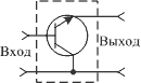
Figure 2 Functional diagram of the inclusion of the transistor with a common collector
In this diagram, the dotted line shows the boundaries of the amplifier shown in Figure 1. It does not show the power supply of the transistor. Given that the power source has zero resistance for alternating current, connecting the output of the transistor to a power source (voltage regulator) is equivalent to connecting to a common wire. The main advantage of an amplifier with a common collector is its large input impedance, so a circuit with a common collector is usually used at low frequencies. Associated with this is the choice of the power circuit of the transistor. To supply the transistor in a circuit with a common collector, current-stable circuits are commonly used: and. The calculation of the resistors included in these circuits does not depend on the switching circuit of the transistor and for the circuit with a common collector it is carried out in the same way as for. The common-collector circuit does not invert the signal and does not amplify it by voltage, so it is often called an emitter follower. Figure 3 shows the principal on a bipolar npn transistor, made according to the common-collector circuit.
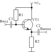
Figure 3 Wiring diagram of the transistor with a common collector (collector stabilization)
In this scheme, R2 is simultaneously a load resistor and a collector stabilization element. The fact that the resistor is connected to the emitter of the transistor does not change the situation. The collector current still flows through this resistor and the voltage drop is applied to the emitter of the transistor. The depth of the DC feedback is determined by the ratio of the resistance of the resistor R1 and the input resistance of the transistor.
The scheme of the cascade with a common collector and emitter stabilization has the best characteristics in terms of stability parameters. In it, the depth of feedback on direct current approaches 100%. A schematic diagram of the switching on of the transistor with a common collector and emitter stabilization is shown in Figure 4.
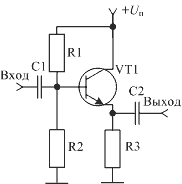
Figure 4 Wiring diagram of the transistor with a common collector (emitter stabilization)
A distinctive feature of the circuit with a common collector is a high input resistance. It can be determined by a formula similar to formula (4). However, in this case, the resistance of the emitter circuit, which is significantly greater than the internal emitter resistance of the transistor, will be recalculated to the input. r e.
In the diagram shown in Figure 3, as a resistance R This resistor R2 is used, and in the circuit shown in Figure 4, resistor R3 is used. With its nominal 1 kOhm and h 21 e, equal to 100, the input impedance of the transistor will be equal to 100 kΩ! With such a resistance, when calculating the transistor cascade, the influence of the resistance of the bias circuit should be taken into account, since the input current also flows through it. The flow paths of the input current in the circuit with a common collector are shown in Figure 5.
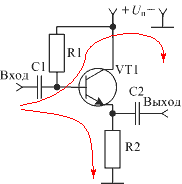
Figure 5 The flow of current through the input circuits of the emitter follower
As can be seen from this scheme, the input current flows not only through the base of the transistor and the resistor R2, but also through the resistor R1, the power source and returns to the signal source. As a result, the input resistance of the emitter follower will be defined as the parallel connection of the input resistance of the transistor and the resistor R1:
For example, when powering the amplifier from a voltage source of 5 V and a collector current of 1 mA, to obtain the maximum dynamic range at the output, you need to set the voltage at the emitter to 2.5 V. Then the resistance R2 = 2.5kΩ, the base current of the transistor ib = 1mA / 100 = 10µA. Resistance R1 = (5V - 2.5V - 0.7V) / 10µA = 180 kΩ. The input impedance of the cascade is Rin = 100kΩ || 180kOm = 64kOhm.
The inherent feedback circuit with OK not only increases the input resistance, but also reduces the output. It can be approximately considered equal to the emitter resistance of the transistor:
More precisely, the output impedance of the circuit with a common collector can be defined as a parallel connection of the emitter resistance of the transistor and resistor R2:
Literature:
Together with the article "The switching circuit of the transistor with a common collector" read:
http: // website / Sxemoteh / ShTrzKask / KollStab /
http: // website / Sxemoteh / ShTrzKask / EmitStab /
Which have not less than three conclusions. In certain situations, they are able to amplify power, generate vibrations or convert a signal. There are many different designs of these devices, and among them is a pnp transistor.
Classify transistors on a semiconductor material. They come from silicon, germanium, etc.
If a transistor of three regions has two hole conductance, it is called a “forward-conducting transistor”, or a “pnp junction transistor”. A device in which two regions have electronic conductivity is called an inverse transistor transistor, or with an npn junction. Both transistors work in the same way, and the difference lies solely in polarity.
Where is the pnp transistor used?
Depending on what characteristics of the transistor, it can be used for various purposes. As already mentioned, the transistor is used to generate, transform and amplify electrical signals. Due to the fact that the input voltage or current changes, the current of the input circuit is controlled. Small changes in the parameters at the input lead to an even greater change in the current and voltage at the output. This amplification property is used in analog technology (radio, communication, etc.).

Nowadays, for analogue technology, there is another, very important industry - digital technology - almost abandoned it and uses only field technology. appeared much earlier than the field one, because in everyday life it is simply called a transistor.
Performance and parameters of transistors
Transistors are structurally manufactured in plastic and metal housings. Given the different purpose of the transistors, these devices are selected according to certain parameters. For example, if you need a transistor to amplify high frequencies, it must have a high frequency gain signal. And if the pnp transistor is used in it must have a high operating collector current.
Reference literature contains the main characteristics of transistors:
- Ik - working (maximum allowable) collector current;
- h21e is the gain;
- Fgr - maximum frequency gain;
- Pk - collector power dissipation.
Phototransistors

A phototransistor is a device that is sensitive to it. In a sealed case of such a transistor, a window is made, for example, from transparent plastic or glass. The radiation through it enters the zone of the phototransistor base. If the base is irradiated, charge carriers are generated. The phototransistor will open when the charge carriers transfer to the collector junction, and the more the base is lit, the more collector current will become.
Without transistors it is impossible to imagine modern electronics. Virtually no serious device can do without them. Over the years of application and improvement transistors have changed significantly, but the principle of their work remains the same.
There are two main types of transistors - bipolar and field. Bipolar transistors are made of doped materials and can be of two types - NPN and PNP. The transistor has three outputs, known as emitter (E), base (B) and collector (K). The figure below shows the NPN transistor where, with the main operating modes (active, saturation, cutoff), the collector has a positive potential, the emitter is negative, and the base is used to control the state of the transistor.
The NPN transistor has one P region enclosed between two N regions:
 |
The junctions between the N and P regions are similar to transitions in the diodes, and they can also be with direct and reverse displacement of the p – n junction. These devices can operate in different modes depending on the type of offset:
- Cutoff: work in this mode also occurs when switching. There is no current between the emitter and the collector, practically “open circuit”, then there is “contact open”.
- Active mode: the transistor operates in the amplifier circuits. In this mode, its characteristic is almost linear. A current flows between the emitter and the collector, the value of which depends on the value of the bias voltage (control) between the emitter and the base.
- Saturation: works when switching. Almost “short circuit” occurs between the emitter and the collector, that is, the “contact is closed”.
- Inverse active mode: as in the active, the current of the transistor is proportional to the base current, but flows in the opposite direction. Used very rarely.
In an NPN transistor, a positive voltage is applied to the collector to create a current from the collector to the emitter. In a PNP transistor, a positive voltage is applied to the emitter to create a current from the emitter to the collector. In NPN, the current flows from the collector (K) to the emitter (E):
It is clear that the directions of current and voltage polarity in PNP and NPN are always opposite to each other. NPN transistors require power with positive polarity relative to common terminals, while PNP transistors require negative power.
PNP and NPN work almost identically, but their modes differ due to polarities. For example, to convert NPN to saturation mode, U B must be higher than U K and U E. Below is a brief description of the modes of operation, depending on their voltage:
 |
The basic principle of operation of any bipolar transistor is to control the base current for controlling the flow of current between the emitter and collector. The principle of operation of NPN and PNP transistors is the same. The only difference is the polarity of the voltages applied to their N-P-N and P-N-P junctions, that is, to the emitter-base-collector.
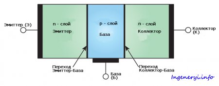
Bipolartransistor - three-electrode semiconductor deviceone of types transistor. Electrodes are connected to three consecutive layers of a semiconductor with alternating type impurity conductivity. By this method of alternation npn and pnp transistors ( n (negative) - electronic type of impurity conductivity, p (positive) - hole). In a bipolar transistor, unlike field effect transistor, charges are simultaneously used two types, carriers of which are electrons and holes (from the word "bi" - "two"). A schematic of the transistor is shown in the second figure.
The electrode connected to the center layer is called baseelectrodes connected to the outer layers are called collector and emitter. In the simplest scheme, the differences between the collector and the emitter are not visible. In reality, the main difference between the collector is a larger area. Pn junction. In addition, for the operation of the transistor requires a small thickness of the base.
Device and principle of operation
Simplified cross section of a bipolar NPN transistor
The first transistors were made based on germany. Currently, they are made mainly from silicon and gallium arsenide. Gallium arsenide-based transistors are used in ultrafast logic circuits and in high-frequency amplifier circuits.
The bipolar transistor consists of three different ways. doped semiconductor layers: emitter Ebase B and collector C. Depending on the type of conductivity, these zones are distinguished. NPN (emitter - nsemiconductor base - p- semiconductor, collector - nsemiconductor) and PNP transistors. Conductive non-rectifying contacts are connected to each of the zones. The base is located between the emitter and the collector and is lightly alloyed, therefore it has a large ohmic resistance. The total base-emitter contact area is much smaller than the collector-base contact area (this is done for two reasons: a large collector-base transition area increases the likelihood of capturing minority carriers from the base to the collector, and since the transfer mode collector-base is normally switched on reverse bias, which increases heat dissipation, contributes to heat removal from the collector), so the bipolar transistor of a general form is an asymmetric device (it is impractical by changing the polarity of the connection swap emitter and collector and get a result similar to the original bipolar transistor - the inverse inclusion).
In the active amplifier mode, the transistor is turned on so that its emitter junction shifted in the forward direction (open), and the collector junction is shifted in the opposite direction (closed). For definiteness, consider npn the transistor, all reasoning is repeated absolutely similarly for the case pnp transistor, with the replacement of the word "electrons" by "holes" and vice versa, as well as the replacement of all voltages with opposite sign. AT npn the transistor electrons, the main current carriers in the emitter, pass through the open transition emitter-base ( are injected) to the base area. Part of these electrons recombines with the main charge carriers in the database (holes). However, due to the fact that the base is made very thin and relatively weakly doped, most electrons injected from the emitter diffuse into the collector region . A strong electric field of a reverse biased collector junction captures minority carriers from the base (electrons), and transfers them to the collector. The collector current is thus almost equal to the emitter current, except for a small recombination loss in the base, which forms the base current ( I uh = I b + I to). Coefficient α, connecting emitter current and collector current ( I to = α I uh) is called the emitter current transfer coefficient. The numerical value of the coefficient α 0,9-0,999. The greater the coefficient, the more efficiently the transistor transmits current. This coefficient is little dependent on the collector-base voltage and base-emitter. Therefore, in a wide range of operating voltages, the collector current is proportional to the base current, the proportionality coefficient is β = α / (1 - α), from 10 to 1000. Thus, a low base current can be controlled by a much higher collector current.
There are three main switching circuits for transistors. In this case, one of the electrodes of the transistor is a common point of entry and exit of the cascade. It must be remembered that the input (output) is understood as the points between which the input (output) alternating voltage acts. Basic inclusion schemes are called common emitter (OE), common base (ON) and common collector (OK) circuits.
Scheme with a common emitter (OE). This scheme is shown in Figure 1. In all the books it is written that this scheme is the most common, because it gives the greatest gain in power.
Fig. 1 - Wiring diagram of a common emitter transistor
The enhancement properties of the transistor characterizes one of its main parameters — the static base current transfer coefficient or the static current gain factor ?. Since it must characterize only the transistor itself, it is determined in the no-load mode (R к = 0). Numerically, it is equal to:
when U to-e = const
This coefficient is equal to tens or hundreds, but the real coefficient k i is always less than ?, since when the load is turned on, the collector current decreases.
The gain of the cascade voltage k u is equal to the ratio of the amplitude or effective values of the output and input AC voltage. The input is the alternating voltage u b-e, and the output is the alternating voltage on the resistor, or, equivalently, the collector-emitter voltage. The base-emitter voltage does not exceed a few tenths of a volt, and the output voltage reaches a few tens of volts (with sufficient load resistance and a source voltage of E 2). It follows that the gain of the cascade in power is equal to hundreds, thousands, and sometimes tens of thousands.
An important characteristic is the input resistance R in, which is determined by Ohm's law:
and is usually from hundreds of ohms to a few kilo. The input impedance of the transistor when turned on according to the OE scheme, as can be seen, is relatively small, which is a significant drawback. It is also important to note that the cascade according to the OE scheme reverses the voltage phase by 180 °
The advantages of the OE scheme include the convenience of feeding it from one source, since the supply voltage of the same sign is applied to the base and collector. The disadvantages include the worst frequency and temperature properties (for example, in comparison with the OT scheme). As the frequency increases, the gain in the OE circuit decreases. In addition, the cascade according to the OE scheme with amplification introduces significant distortions.
The scheme with a common base (OB). Scheme OB is depicted in Figure 2.
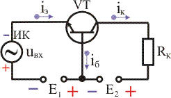
Fig. 2 - Switching circuit of a common base transistor
Such an inclusion scheme does not give a significant gain, but has good frequency and temperature properties. It is not used as often as the OE scheme.
The current gain of the ON circuit is always a bit less than one unit:
since the collector current is always only slightly less than the emitter current.
Is the static current transfer ratio for the ON circuit indicated? and is determined by:
with u K = const
This coefficient is always less than 1 and the closer it is to 1, the better the transistor. The voltage gain is the same as in the OE circuit. The input impedance of the circuit OB is ten times lower than in the OE circuit.
For the circuit ON, the phase shift between the input and output voltage is absent, that is, the phase of the voltage does not turn over during amplification. In addition, when amplifying, the OT circuit introduces much less distortion than the OE circuit.
Scheme with a common collector (OK). The switching circuit with a common collector is shown in Figure 3. This scheme is often called the emitter follower.
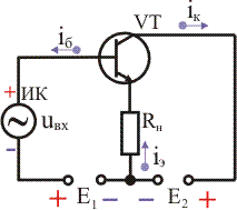
Fig. 3 - Wiring diagram of the transistor with a common collector
The peculiarity of this circuit is that the input voltage is completely transferred back to the input, that is, negative feedback is very strong. The current gain is almost the same as in the OE circuit. The voltage gain approaches unity, but is always less than it. As a result, the power gain is approximately equal to k i, i.e. several dozens.
In the circuit OK, there is no phase shift between the input and output voltage. Since the voltage gain is close to unity, the output voltage in phase and amplitude coincides with the input voltage, i.e. it repeats it. That is why this scheme is called an emitter follower. Emitter - because the output voltage is removed from the emitter relative to the common wire.
The input resistance of the circuit is quite high (tens of kilo-ohms), and the output is relatively small. This is an important advantage of the scheme.