A low frequency amplifier (ULF) is such a device for amplifying electrical oscillations corresponding to the frequency range heard by the human ear, ie, ULF should be amplified in the frequency range from 20 Hz to 20 kHz, but some VLF can have a range to 200 kHz. ULF can be assembled as a standalone device, or used in more complex devices - televisions, radios, radio, etc.
The peculiarity of this circuit is that the 11 output of the TDA1552 chip controls the operating modes - Normal or MUTE.

C1, C2 - pass-through blocking capacitors, used to cut off the constant component of the sinusoidal signal. Electrolytic capacitors are best not to use. The TDA1552 chip should be placed on the radiator using heat-conducting paste.
In principle, the presented circuits are bridge ones, since the TDA1558Q has 4 amplification channels in one case of the TDA1558Q microassembly, therefore, pins 1–2 and 16–17 are connected in pairs, and the input signals of both channels go through capacitors C1 and C2. But if you need silica gel on four columns, then you can use the option of the scheme below, although the power will be 2 times less per channel.
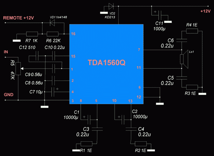
The basis of the design is micro assembly TDA1560Q class H. The maximum power of such a ULF reaches 40 W, with a load of 8 Ohms. This power is provided by an increased voltage of about two times, due to the work of the capacitors.
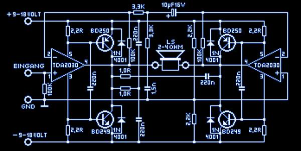
The output power of the amplifier in the first circuit assembled on the TDA2030- 60W with a load of 4 Ohms and 80W with a load of 2 Ohms; TDA2030A 80W with a load of 4 Ohms and 120W with a load of 2 Ohms. The second scheme of the considered ULF is already with an output power of 14 watts.
This is a typical two channel ULF. With a small strapping of passive radio components on this chip, you can assemble an excellent stereo amplifier with an output power of 1 W on each channel.
Micro Assembly TDA7265 - is a fairly powerful dual-channel Hi-Fi amplifier class AB in a typical Multiwatt package, the microcircuit has found its niche in high-quality stereo technology, Hi-Fi class. Simple wiring diagrams and excellent parameters made the TDA7265 perfectly balanced and a great solution when building amateur radio high-quality audio equipment.
Micro assembly is a class AB quad amplifier, designed specifically for use in car audio devices. On the basis of this chip, you can build several qualitative variants of ULF using a minimum of radio components. The microcircuit can be advised to novice radio amateurs for home assembly of various acoustic systems.
The main advantage of the amplifier circuit on this microassembly is the presence of four channels independent of each other. This power amplifier works in AB mode. It can be used to enhance various stereo signals. If desired, you can connect to the speaker system of the car or personal computer.
The TDA8560Q is just a more powerful analog of the well-known TDA1557Q radio amateur. The developers only increased the output stage, thanks to which the ULF is well suited to two ohm loads.
The LM386 microassembly is a ready-made power amplifier that can be used in low voltage supply designs. For example, when powering the circuit from the battery. The LM386 has a voltage gain of about 20. But by connecting external resistances and capacitances, you can adjust the gain to 200, and the output voltage automatically becomes half the power supply.
The LM3886 microassembly is a high quality amplifier with an output power of 68 watts at 4 ohms load or 50 watts at 8 ohms. At the peak moment, the output power is capable of reaching 135 watts. A wide voltage range from 20 to 94 volts is applicable to the microcircuit. And you can use both bipolar and unipolar power supplies. The harmonic coefficient of ULF is 0.03%. And it is all over the frequency interval from 20 to 20,000 Hz.

The circuit uses two integrated circuit ICs - the KR548UH1 as a microphone amplifier (installed in the tangent) and (TDA2005) in a bridge-in as a terminal amplifier (installed in the case of the system instead of the motherboard). As an acoustic emitter, a secondary alarm system with a magnetic head alarm is used (piezo emitters are not suitable). Processing consists of breaking up the syringe and throwing out a personal tweeter with an amplifier. Microphone - electrodynamic. When using an electronic microphone (for example, from Chinese telephone pipes), the connection point of the microphone with a condenser must be connected through a ~ 4.7K resistor to + 12V (after the button!). The 100K resistor in the K548UH1 feedback circuit is better to be supplied with resistance ~ 30-47K. This resistor is used to adjust the volume. Chip TDA2004 is better to install on a small radio.
Test and operate - with the emitter under the hood, and the tangent in the cabin. Otherwise, screaming due to self-excitation is inevitable. The subresistor resistor sets the volume level so that there is no strong sound distortion and self-excitation. In case of insufficient volume (for example, a poor microphone) and a clear power margin of the emitter, the gain of the microphone amplifier can be increased by increasing the counterpart in the feedback circuit several times (the one according to the 100K scheme). In an amicable way, one more primembas would be needed, which does not allow the circuit to self-excite - any phase-shifting chain or filter at the excitation frequency. Although the scheme works fine without complications
After mastering the basics of electronics, the beginner radio amateur is ready to solder his first electronic structures. Audio power amplifiers are usually the most repeatable designs. There are a lot of schemes, each is different in its parameters and design. In this article several simplest and fully working amplifier circuits will be considered, which can be successfully repeated by any amateur radio. The article does not use complex terms and calculations, everything is simplified as much as possible so that no additional questions arise.
Let's start with a more powerful scheme.
So, the first circuit is made on a well-known TDA2003 chip. This is a mono amplifier with an output power of up to 7 watts per load of 4 ohms. I want to say that the standard circuit for the inclusion of this microcircuit contains a small number of components, but a couple of years ago I had invented a different circuit on this microcircuit. In this scheme, the number of components is minimized, but the amplifier has not lost its sound parameters. After the development of this circuit, all its amplifiers for low-power speakers began to do it on this circuit.
The scheme of the presented amplifier has a wide reproducible frequency range, the supply voltage range is from 4.5 to 18 volts (typical 12-14 volts). The microcircuit is installed on a small heat sink, since the maximum power reaches up to 10 watts.
The microcircuit is capable of operating at a load of 2 ohms, which means that 2 heads with a resistance of 4 ohms can be connected to the output of the amplifier.
The input capacitor can be replaced by any other, with a capacity of from 0.01 to 4.7 microfarads (preferably from 0.1 to 0.47 microfarads), you can use both film and ceramic capacitors. All other components, it is desirable not to replace.
Volume control from 10 to 47 kOhm.
The output power of the chip allows it to be used in low-power PC speakers. It is very convenient to use a chip for autonomous speakers to a mobile phone, etc.
The amplifier works immediately after switching on, does not need additional adjustment. It is advised to connect the power supply minus to the heat sink. All electrolytic capacitors are preferably used at 25 volts.
The second circuit is assembled on low-power transistors, and is more suitable as a headphone amplifier.
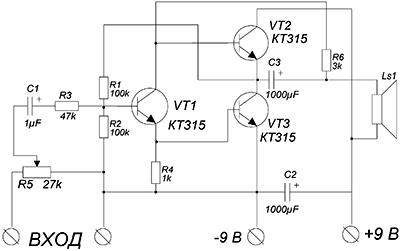
This is probably the highest quality scheme of this kind, the sound is clear, the whole frequency spectrum is felt. With good headphones, it feels like you have a full subwoofer.
The amplifier is assembled on only 3 reverse transistors, as the cheapest option, KT315 series transistors were used, but their choice is quite wide.
The amplifier can operate on a low-impedance load, up to 4 Ohms, which makes it possible to use the circuit to amplify the signal of a player, radio, etc. As the power source used battery type krone with a voltage of 9 volts.
In the final cascade also used transistors KT315. To increase the output power, you can use KT815 transistors, but then you have to increase the supply voltage to 12 volts. In this case, the power of the amplifier will reach up to 1 Watt. The output capacitor can have a capacity of 220 to 2200 microfarads.
Transistors in this circuit do not heat up, therefore, any cooling is not necessary. When using more powerful output transistors, you may need small heat sinks for each transistor.
And finally - the third scheme. Presented at least a simple but proven version of the structure of the amplifier. The amplifier is capable of operating from undervoltage up to 5 volts; in this case, the output power of the PA will be no more than 0.5 W, and the maximum power at 12 volts reaches up to 2 Watts.
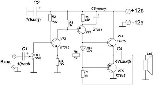
The output stage of the amplifier is built on a domestic complementary pair. Adjust the amplifier selection of the resistor R2. For this, it is advisable to use a trimmer to 1kOhm. Slowly turn the regulator until the quiescent current of the output stage is 2-5 mA.
The amplifier does not have a high input sensitivity, so it is advisable to use a preamplifier in front of the input.
A diode plays a significant role in the circuit, it is here to stabilize the output stage mode.
The output stage transistors can be replaced by any complementary pair of relevant parameters, for example KT816 / 817. An amplifier can power low-powered stand-alone speakers with a load impedance of 6-8 ohms.
Amplifier unit amateur radio complex
The main technical characteristics of the power amplifier:
Rated output power, W, .......................... 2x25 (2x60)
Power bandwidth, kHz ........................................... 0.02 ... 150 (100)
Rated input voltage, V .................................... 1 (1)
Harmonic coefficient,%, at frequency, kHz:
1 .............................................................................. 0,1(0,1)
2 ............................................................................ 0,14(0,55)
10 ............................................................................ 0,2(0,9)
20 ............................................................................. 0,35(1,58)
The coefficient of intermodulation distortion,%, ......... 0.3 (0.47)
Input impedance, kΩ .................................................... 150
Quiescent current of the output stage, mA ........................................ 50 (50 )
Cascade of voltage signal amplification is made at OU A1. As can be seen from the diagram, a part of the output signal is supplied to the power supply circuit through the R6C3C4R4R5 circuit (together with the V6 and V7 zener diodes, elements of this circuit, in addition to the R6 resistor, provide stabilization and filtering of the supply voltages). As a result, the voltage at the power supply terminals of the OS at the maximum signal is shifted (relative to the common wire) in the corresponding direction and the range of the output signal of the OS increases significantly. Large in-phase signals that appear at the inputs of an op amp do not pose a danger, since op amp suppresses them well (typical attenuation coefficient is 70 ... 90 dB). When a signal is applied to the inverting input, the stabilized supply voltages should not exceed + -28 V, on the inverting inputs - values equal to (11Вх + 28 V), where 11вх is the amplitude of the input signal. Unused input in any case must be connected to the common wire. OU K140UD8A in power amplifiers can be replaced by K140UD8B, K140UD6, K140UD10, K140UD11, K544UD1. The worst results are given by the use of OU K140UD7. It is not recommended to use OU K140UD1B, K140UD2A, K140UDDB, K153UD1. Instead of the KS518A stabilitrons, it is possible to use connected in series Zener diodes D814A, D814B with a total stabilization voltage of about 18V.
High quality ULF
The amplifier described below is suitable for amplifying high-power audio signals as part of high-end sound-reproducing devices, as well as for use as a powerful broadband operational amplifier.
Main technical characteristics of the amplifier:
Nominal output power, W, with load resistance,
Ohm: 8 ............................................... ........................................... 48
4..........................................................................................60
The range of reproducible frequencies with non-uniformity of the frequency response is not more than 0.5 dB and an output power of 2 W, Hz .................. 10 ... 200000
Distortion factor at rated power
in the range of 20 ... 20000 Hz,% ........................................ ............ 0.05
Rated input voltage, V .................................. 0.8
Input impedance, kΩ .................................................... ........ 47
Output impedance, Ohm .............................................. .... 0.02
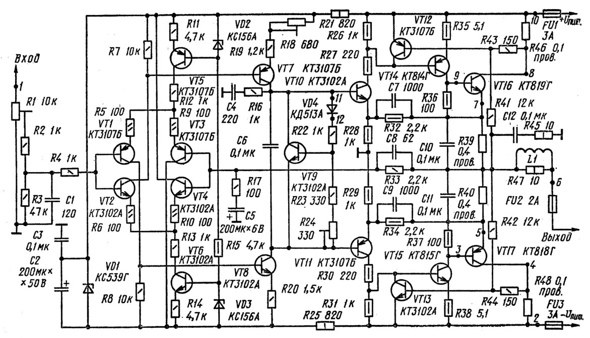
The input stage of the amplifier consists of two differential amplifiers (connected in parallel), performed on transistors VT1, VT3 and VT2, VT4 of the opposite structure. Current generators on transistors VT5, VT6 ensure the stability of the values (about 1 mA) of the total emitter currents of the differential pairs, as well as isolation in power supply circuits. The signal to the output amplifier is supplied from controlled current generators (VT7, VT7), which operate in antiphase. Such an inclusion has doubled the “buildup” current, reduced nonlinear distortion, and improved the frequency properties of the amplifier as a whole. Each of the arms of the symmetric output amplifier is made according to the Darlington scheme, and is a three-stage amplifier (in two stages the transistors are connected according to the scheme with a common emitter and in one with a common collector). The amplifier is covered by frequency-dependent OOS, which determines its voltage transmission coefficient, which is close to three in the audio range. Since the feedback signal taken from the resistor R39 (R40) is proportional to changes in the current of the output transistor, a rather rigid stabilization of the operating point of this transistor is additionally carried out. The bias voltage of the output stage is determined by the resistance of the collector-emitter junction of the transistor VT9 and is controlled by the resistor R24. The bias voltage is thermally stabilized by a VD4 diode, which is attached to the heat sink of one of the high-power transistors.
The correction elements R16, C4, C6 - C11 ensure the stability of the amplifier and equalize its frequency response. R2C1 passive low pass filter prevents RF signals from entering the input. Chain C12R45L1R47 compensates for the reactive component of the load resistance. On transistors VT12 and VT13 assembled node protection output transistors against overload current and voltage. Resistor R1 allows, if necessary, to limit the output power in accordance with the level of the signal from the preamplifier and the capabilities of the loudspeaker used.
In the amplifier, you can use other low-power high-frequency silicon transistors, such as KT342A, KT342B and KT313B, KT315 and KT361 (with indices from B to E). Transistors VT14 and VT15 (possible replacement - KT816V, KT816G and KT817V, KT817G or KT626V and KT904A) are equipped with ribbed heat sinks with dimensions of 23x25x12 mm. As an output, you can apply the KT818GM and KT819GM transistors, which allow you to get power over 70 watts with increasing supply voltage. Zener VD1 can also be D816G or 2С536А, VD2 and VD3 - КС147А (with corresponding correction of resistances of resistors R11 and R14).
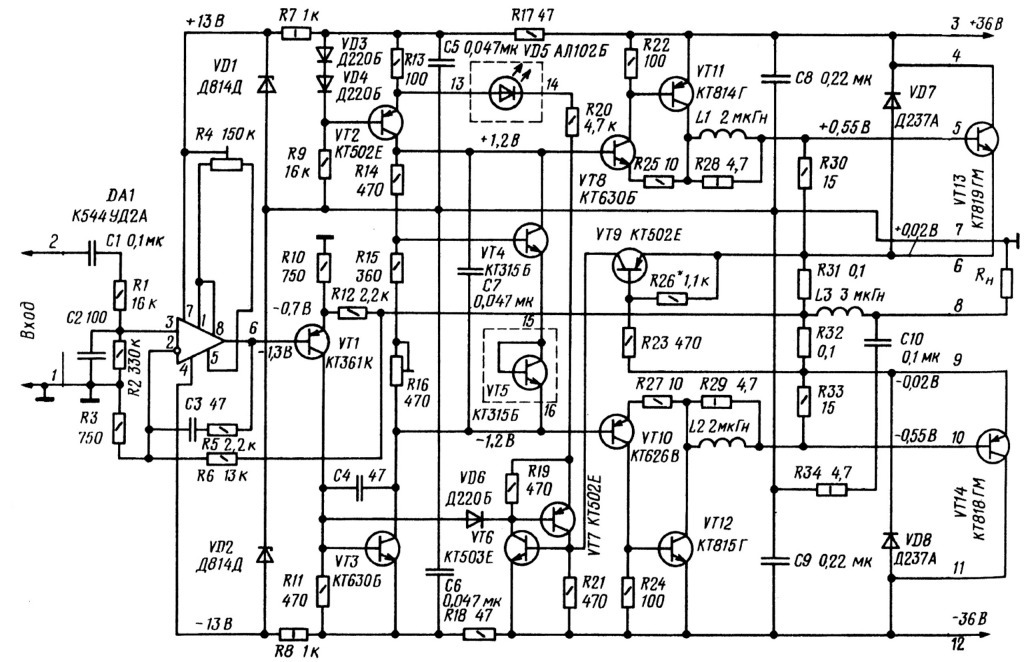
Power Amplifier
Rated (maximum) power, W ..................... 60 (80)
Nominal frequency range, Hz ................................ 20 ... 20000
Harmonic coefficient in the nominal frequency range,% 0.03
Rated input voltage, V ................................... 0.775
Output impedance, Ohm, not more ................................ 0.08
The slew rate of the output voltage, V / µs ............. 40
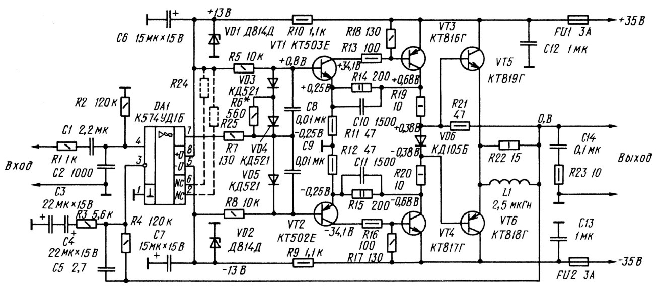
The main voltage gain provides a cascade at the high-speed op amp DA1. The pre-final amplifier stage is built on VT1 - VT4 transistors. Unlike the prototype, an output emitter follower, made on VT5, VT6 transistors operating in the "B" mode, is added to the described amplifier. Temperature stability is achieved by including in the collector circuit of transistors VT3, VT4 of resistors a relatively large resistance R19, R20. Each shoulder of the pre-terminal cascade is covered by a local DUS circuit with a depth of at least 20 dB. OOS voltage is removed from the collector loads of transistors VT3, VT4 and through dividers R11R14 and R12R15 is fed to the emitter circuit of transistors VT1, VT2. Frequency correction and stability in the OOS circuit is provided by the capacitors CU, C11. Resistors R13, R16 and R19, R20 limit the maximum currents of the pre-terminal and terminal stages of the amplifier during a short circuit load. For any overloads, the maximum current of transistors VT5, VT6 does not exceed 3.5 ... 4 A, and in this case they do not overheat, since the fuses FU1 and FU2 have time to burn out and disconnect the power supply to the amplifier.
Reducing the harmonic ratio is achieved by introducing deep (at least 70 dB) total OOS, the voltage of which is removed from the amplifier output and through the C3C5R3R4 divider is fed to the inverting input of the op-amp DA1. Capacitor C5 adjusts the frequency response of the amplifier in the circuit of OOS. The circuit R1C1 included at the input of the amplifier limits its bandwidth to 160 kHz. The maximum possible linearization of AHHUMZCH in the band of 10 ... 200 Hz is achieved by an appropriate choice of capacitors C1, C3, C4.
Instead of those indicated on the circuit, it is possible to use OU K574UDD1A, K574UDD1V and transistors of the same types as in the circuit, but with indices D, D (VT1, VT2) and B (VT3 - VT6).
UMZCH with the output cascade on field-effect transistors
Main technical characteristics:
Rated (maximum) output power, W. 45 (65)
Harmonic factor,%, not more than, .................................... 0.01
Rated input voltage, mV ............................ 775
Nominal frequency range, Hz, ......................... 20 ... 100000
The slew rate of the output voltage, V / µs, ................ 60
S / N ratio, dB ............................................ ......... 100
The input stage of the amplifier is made on the op-amp DA1. In order to increase the amplitude of the output voltage, control of the output transistors of the UMZCH is applied over the power supply circuits of the OS. The output signal is removed from the positive power output of DA1 and through the ON transistor VT1 connected to the circuit with ON is supplied to one of the inputs of the differential cascade on transistors VT2, VT4. At its second input comes a stabilized voltage from the divider formed by the diodes VD2 - VD5 and the resistor R13.
The described amplifier does not require any special measures to protect the output transistors from short circuits in the load, since the maximum voltage between the source and the gate is only twice as high as the rest voltage and corresponds to the current through the output transistor about 9 A. Such current applied transistors reliably withstand for as long as it takes to blow out the fuses and disconnect the AMC from the power source.
Coil L1 is wound in a single layer on a toroidal frame with an outer diameter of 20, inner 10 and a height of 10 mm and contains 28 turns of wire sew-2 1.0.
In UMZCH, it is desirable to use OU KR544UDD2A, as the most broadband domestic OU with internal frequency correction. KT3108A transistors are interchangeable KT313A, KT313B, and KP912B - KP912A and KP913, KP920A. 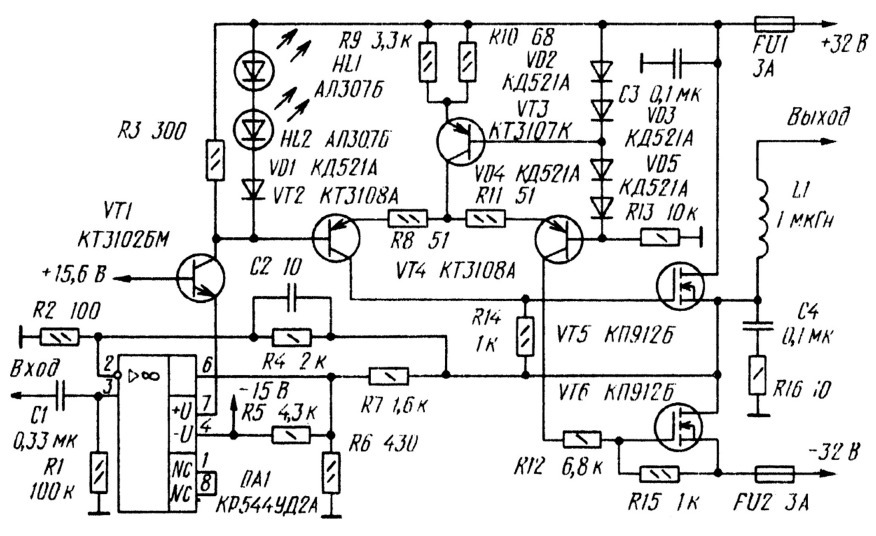
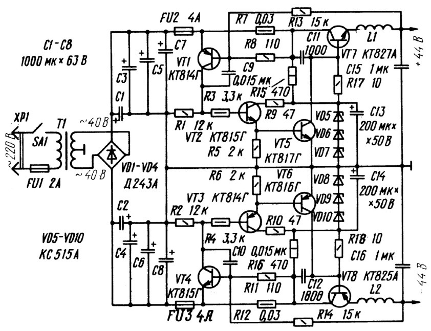
High quality power amplifier
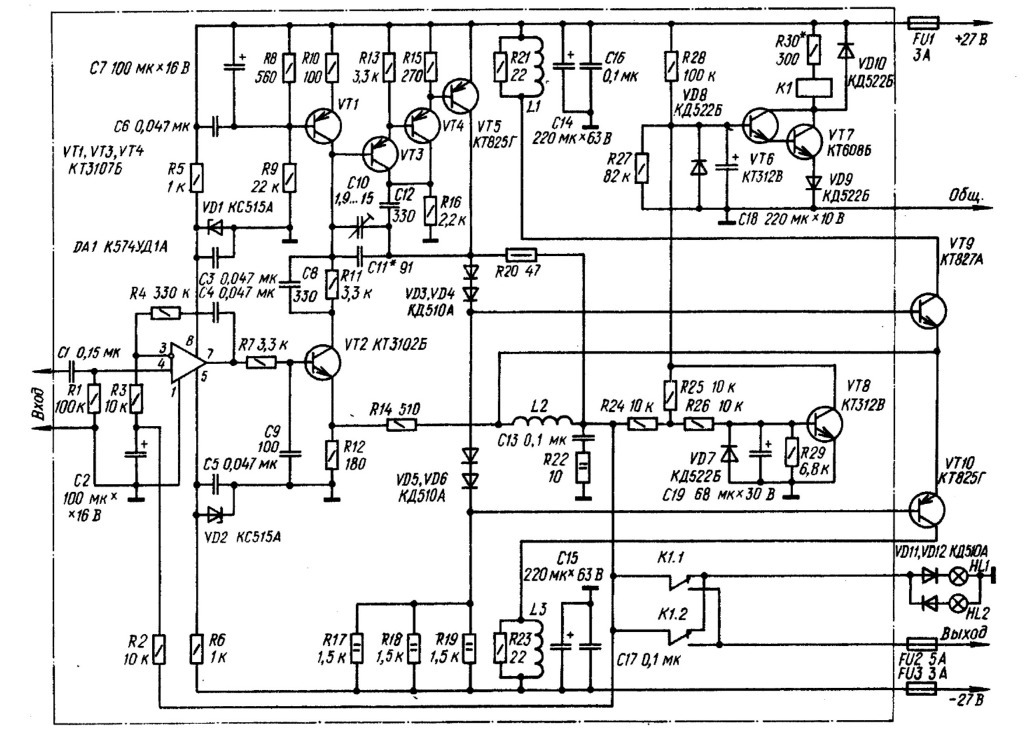
When designing the amplifier described below, the "Kvod-405" amplifier was taken as the basis, successfully combining high technical characteristics and circuit simplicity. The block diagram of the amplifier basically remained unchanged; only devices for protecting the transistors of the output stage against overload were excluded. Practice has shown that devices of this kind do not completely eliminate the failures of transistors, but often they introduce nonlinear distortions at maximum output power. The current transistors can be limited and otherwise, for example, using overcurrent protection in voltage regulators. At the same time, it seems appropriate to protect the loudspeakers in case of failure of the amplifier or power sources. To improve the symmetry of the amplifier, the output stage is performed on a complementary pair of transistors, and to reduce nonlinear distortions such as a “step” between the bases of transistors VT9, VT10, diodes VD5, VD6 are included. This ensures sufficiently reliable closing of the output stage transistors in the absence of a signal. Slightly modified input circuit. The non-inverting input of the OA DA1 was used as a signal, which made it possible to increase the input impedance of the amplifier (it is determined by the resistance of resistor R1 and is equal to 100 kOhm.) It should be noted, however, that in the non-inverting variant the stability of the amplifier remains high. A simple, well-proven device (VT6 - VT8) used in the industrial amplifier "Brig - 001" was used to prevent clicks in loudspeakers caused by transients during power up, as well as to protect loudspeakers from DC voltage when an amplifier or power supply fails. ". When this device triggers, one of the lamps HL1, HL2 lights up, signaling that there is a constant voltage of one or another polarity at the output of the amplifier. Basically, the circuit of the described amplifier does not differ from the amplifier circuit "Acquisition -405". The coils are wound with wire sew-2 1.0 on frames with a diameter of 10 mm and contain: L1 and L3 - 50 turns each (inductance - 5 ... 7 μH), L2 - 30 turns (3 μH).
Instead of the ones shown on the diagram in the amplifier, it is possible to use OU K574UDD1B, K574UDD1V, K544UDD2, and also (with some deterioration of the parameters) K544UD1 and K140UD8A - K140UD8V; transistors KT312V, KT373A (VT2), KT3107B, KT3107I, KT313B, KT361V, KT361K (VT1, VT3, VT4), KT315V (VT6, VT8), KT801A, KT801B (VT7). Each of the transistors KT825G can be replaced with composite transistors KT814V, KT814G + KT818V, KT818G, and KT827A with composite transistors KT815V, KT815G + KT819V, KT819G. Diodes VD3 - VD6, VD11, VD12 - any silicon with a maximum direct current of at least 100 mA, VD7 - VD10 - the same, but with a maximum current of at least 50 mA. In the absence of Zener KS515A, it is permissible to use D814A, D814B or KS175A zener diodes connected in series.
Maximum output power, W, at a load of 4 ohms ..... 2x70
Rated input voltage, V ................................... 0.2
Upper bound of frequency range, kHz .................................... 50
The slew rate of the output voltage, V / µs .............. 5.5
Signal-to-noise ratio (unweighted), dB ............................... 80
Harmonic factor,%, not more than, ........................................ 0, 05
Amplifier with multiloop OOS
Main technical characteristics:
Nominal frequency range, Hz, ................................ 20 ... 20000
Nominal load resistance, Ohm ................................... 4
Rated (maximum) output power, W, with load resistance, Ohm:
4 .................................................................................. 70(100)
8 ........................................................................................40(60)
Frequency range, Hz, ............................................. ........ 5 ... 100000
The slew rate of the output voltage, V / µs, at least ... 15 Harmonic factor,%, not more than, at a frequency, Hz:
20...5000 .................................................................................. 0,001
10000 ................................................................................ 0,003
20000 ................................................................................. 0,01
Harmonic factor,%, not more than, ...................................... 0.01
Rated input voltage, V .......................................... 1
Input resistance, kOhm, not less, ...................................... 47
The first stage is assembled on an DA1 operational amplifier (OA), the rest are on transistors (the second and third are on VT1, VT3, respectively, the fourth on VT8, VT11 and VT10, VT12, the fifth on VT13, VT14). In the fourth (pre-terminal) cascade, transistors of different structure were used, connected according to the composite emitter follower circuit, which allowed local OOS to be introduced into it and thus increased linearity and reduced output resistance. To reduce transient distortion at high frequencies, the output stage operates in AB mode, and the resistance of the bias resistors (R30, R33) is limited to 15 Ohms. All transistor amplifier cascades are covered by a circuit of local environmental protection with a minimum depth of 50 dB. OOS voltage is removed from the output of the amplifier and through the divider R10R12 is fed to the emitter circuit of the transistor VT1. Frequency correction and stability in the OOS circuit are provided by the capacitor C4. The introduction of local environmental protection allowed even for the most unfavorable combinations of the amplifying properties of transistors to limit the harmonics of this part of the amplifier to 0.2%. The protection device consists of a trigger on transistors VT6, VT7 and a threshold element on the transistor VT9. As soon as the current through any of the output transistors exceeds 8 ... 9 A, the transistor VT9 opens, and its collector current opens the trigger transistors VT6, VT7.
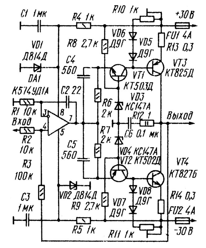
Power Amplifier
The RF amplifier offered to the attention of radio amateurs has very low harmonic and intermodulation distortion factors, it is relatively simple, able to withstand a short-term short circuit in the load, does not require remote elements to thermally stabilize the current of the output stage transistors.
Main technical characteristics:
Maximum power at a load of 4 ohms, W ........................... 80
Nominal frequency range, Hz ................................... 20 .... 20000
Harmonic coefficient with a maximum output power of 80 W,%, at a frequency of:
1 kHz ................................................ ................................. 0.002
20..................................................................................... 0,004
Intermodulation distortion factor,% .................. 0.0015
The slew rate of the output voltage, V / µs .................... 40
To increase the input impedance, transistors VT1, VT2 are introduced into the amplifier. This facilitated the operation of the OA DA1 and allowed to provide a stable voltage base - emitter of the transistors VT3, VT4 when the temperature changes.
Resistor R14 is set symmetry shoulders of the output stage of the amplifier. 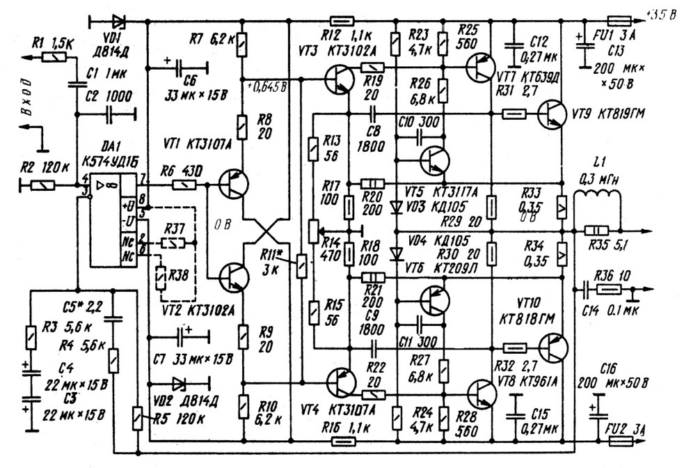
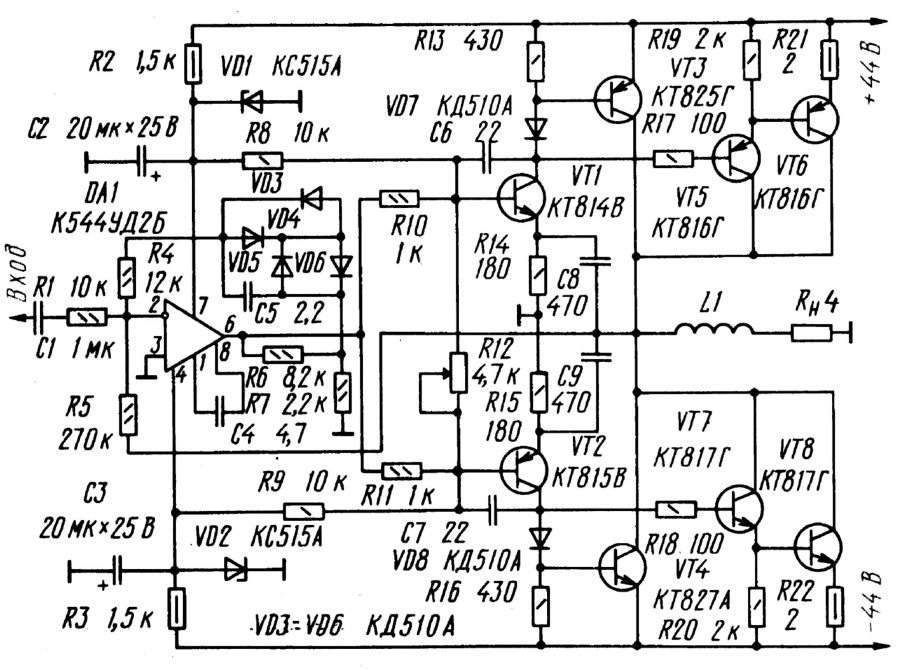
Simple power amplifier
Main technical characteristics:
Input Voltage, V .............................................. ................ 1,8
Input impedance, kΩ .................................................... .......ten
Rated output power, W, ....................................... 90
Nominal frequency range, Hz ................................ 10 ... 20000
Harmonic coefficient,%, at frequency, Hz:
200 .................................................................................... 0,01
2000 ............................................................................ 0,018
20000 ............................................................................... 0,18
Relative noise level, dB, not more than ......................... -90
The slew rate of the output voltage, V / µs ................. 17
The power amplifier consists of a cascade of voltage amplification at the high-speed op amp DA1 and an output circuit of the transistors VT1 - VT4. The transistors of the complementary pair of the pre-terminal cascade (VT1 - VT2) are connected according to the scheme with a common base, and the terminal (VT3 - VT4) - with a common emitter. Such inclusion of powerful composite transistors of the terminal stage provides the signal amplification not only in current, but also in voltage. The symmetry of the shoulders of the output stage helps to reduce the nonlinear distortion introduced by the amplifier. For the same purpose, it is covered by a common OOS circuit, the voltage of which is removed from the amplifier output and fed through a resistor R3 to the non-inverting input of the op-amp. Capacitors C4, C5, shunt resistors R6, R7 reduce the distortion type "step". The R12C6 circuit prevents the amplifier from self-excitation in the region of higher audio frequencies and increases the stability of its operation under the reactive nature of the load. The gain depends on the ratio of the resistors R2, R3. With the values indicated on the diagram, it is equal to 10.
Any unstabilized bipolar source with voltage of 25 ... 45 V can be used to power the amplifier. Instead of KT503D transistors, you can use KT503E, instead of KT502D - KT502E. The KT827B and KT825D transistors can be replaced with the composite of KT817G + KT819GM and KT816G + KT818GM transistors, respectively.
200 W power amplifier with power supply
Main technical characteristics:
Nominal frequency range, Hz ................................ 20 ... 20000
Maximum output power, W, at a load of 4 ohms ........ 200
Harmonic factor,%, with an output power of 0.5..150 W at a frequency, kHz
1 ..........................................................................................0,1
10 .................................................................................... 0,15
20 .................................................................................... 0,2
Efficiency,% ............................................... .............................................. 68
Rated input voltage, V ............................................ 1
Input impedance, kΩ .................................................... .. ten
The slew rate of the output voltage, V / µs ................... 10
The pre-amplification cascade is made on a high-speed OA DA1 (K544UD2B), which, along with the necessary voltage gain, ensures stable operation of the amplifier with deep environmental protection. Feedback resistor R5 and resistor R1 determine the gain of the amplifier. The output stage is made on transistors VT1 - VT8. Zener diodes VD1, VD2 stabilize the power supply voltage of the OU, which is simultaneously used to create the necessary bias voltage of the output stage. Capacitors C4, C5 are correcting. With increasing capacitance of the capacitor C5, the stability of the amplifier increases, but at the same time nonlinear distortions increase, especially at higher audio frequencies. The amplifier maintains performance while reducing the supply voltage to 25 V.
As a power source, you can use a conventional bipolar power supply, the concept of which Powerful integrated transistors VT7 and VT8, included in the emitter follower circuit, provide a fairly good filtering of the supply voltage ripples with the mains frequency and stabilization of the output voltage due to the ZDs installed in the transistor base circuit - VD10. The elements L1, L2, R16, R17, C11, C12 eliminate the possibility of high-frequency generation. Resistors R7, R12 of the power supply unit are a piece of PEL, PEV-1 or PELSHO copper wire with a diameter of 0.33 and a length of 150 mm wound on the body of the MLT-1 resistor. The power transformer is made on a toroidal magnetic core of electrical steel E320, 0.35 mm thick, a tape width of 40 mm, an internal diameter of the magnetic core 80, and the outer one - 130 mm. The network winding contains 700 turns of wire PELSHO 0.47, secondary - 2x130 turns of wire PELSHO 1.2 mm.
Instead of OU K544UDD2B, you can use K544UD2A, K140UD11 or K574UD1. Each of the KT825G transistors can be replaced with the composite KT814G, KT818G transistors, and the KT827A-composite transistors KT815G, KT819G. Diodes VD3 - VD6 UMZCH can be replaced by any high-frequency silicon diodes, VD7, VD8 - any silicon with a maximum forward current of at least 100 mA. Instead of Zener KS515A, you can use the connected in series Zener D814A (B, C, D, D) and KS512A.
BP