The material of this article is intended not only for the owners of rare TVs who want to restore their working capacity, but also for those who want to understand the circuitry, the device and the principle of the operation of switching power supplies. If you learn the material of this article, then you can easily be, whether it's a TV, a laptop or office equipment. And so we proceed ...
In Soviet-made TVs, the third generation of ZUSTSTS used impulse power supply units - MP (power module).
The switching power supplies, depending on the TV model where they were used, were divided into three modifications - MP-1, MP-2 and MP-3-3. The power modules are assembled according to the same electrical scheme and differ only in the type of the pulse transformer and in the rated voltage of the capacitor C27 at the output of the rectifier filter (see schematic diagram).
Functional scheme and operating principle of the switching power supply of ZUSTST TV
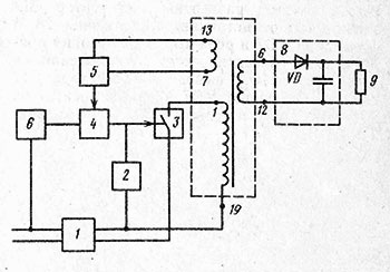
Fig. 1. Functional diagram of the switching power supply of ZUSTST TV:
1 - network rectifier; 2 - the driver of the start pulse; 3 - transistor pulse generator, 4 - cascade control; 5 - stabilization device; 6 - protection device; 7 - impulse transformer of the power supply unit of TV sets 3усцт; 8 - rectifier; 9 - load
Let at the initial moment of time in the device 2 a pulse be formed which will be opened by the transistor of the pulse generator 3. In this case a linearly increasing sawtooth current will flow through the winding of the pulse transformer with the terminals 19, 1. At the same time, in the magnetic field of the transformer core, energy is accumulated, the value of which is determined by the open state of the transistor of the pulse generator. The secondary winding (terminals 6, 12) of the pulse transformer is wound and connected in such a way that during the accumulation of magnetic energy, a negative potential is applied to the anode of the diode VD and it is closed. After a while, the control stage 4 closes the transistor of the pulse generator. Since the current in the winding of the transformer 7 can not instantly change due to the stored magnetic energy, an EMF of self-induction of the opposite sign occurs. The diode VD opens, and the secondary current (terminals 6, 12) rises sharply. Thus, if in the initial period of time the magnetic field was associated with the current that flowed through the winding 1, 19, now it is created by the winding current 6, 12. When all the energy accumulated during the closed state of key 3 goes into the load, in the secondary winding will reach zero value.
From the above example, we can conclude that by adjusting the duration of the open state of the transistor in a pulse generator, it is possible to control the amount of energy that enters the load. This adjustment is carried out using the control stage 4 on the feedback signal - the voltage at the terminals of the winding 7, 13 of the pulse transformer. The feedback signal at the terminals of this winding is proportional to the voltage on the load 9.
If the voltage on the load decreases for some reason, the voltage that goes to the stabilization device 5 also decreases. In turn, the stabilization device through the control cascade will start closing the transistor of the pulse generator later. This will increase the time during which current flows through the winding 1, 19, and accordingly the amount of energy transferred to the load will increase.
The moment of the next opening of the transistor 3 is determined by the stabilization device, where the signal coming from the winding 13, 7 is analyzed, which automatically maintains the average value of the output DC voltage.
The use of a pulsed transformer makes it possible to obtain a different amplitude in the voltage in the windings and eliminates the galvanic connection between the circuits of the secondary rectified voltages and the power supply network. The control stage 4 determines the sweep of the pulses generated by the generator and, if necessary, turns it off. The generator is disconnected when the mains voltage drops below 150 V and the power consumption is reduced to 20 W when the stabilization cascade ceases to function. When the stabilization cascade is not running, the pulse generator turns out to be uncontrollable, which can lead to the generation of large current pulses in it and to the failure of the transistor of the pulse generator.
Schematic diagram of the switching power supply of ZUSTST TV
Consider the circuit diagram of the power module MP-3-3 and the principle of its operation.
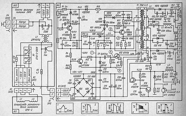
Fig. 2 Schematic diagram of the switching power supply of ZUSTST TV, module MP-3-3
It consists of a low-voltage rectifier (diodes VD4 - VD7), a pulse generator (VT3), a pulse generator (VT4), a stabilization device (VT1), a protection device (VT2), a pulsed transformer T1 of a 3-watt power supply unit and rectifiers on diodes VD12 - VD15 with voltage regulator (VT5 - VT7).
The pulse generator was assembled according to the blocking-generator scheme with collector-base connections on the transistor VT4. When the TV is switched on, the DC voltage from the output of the low-voltage rectifier filter (capacitors C16, C19 and C20) through the winding 19, 1 of the transformer T1 is fed to the collector of the transistor VT4. Simultaneously, the mains voltage from the diode VD7 through the capacitors C11, C10 and the resistor R11 charges the capacitor C7, and also goes to the base of the transistor VT2, where it is used in the device for protecting the power module from the undervoltage of the network. When the voltage across the capacitor C7, applied between the emitter and the base 1 of the unijunction transistor VT3, reaches a value of 3 V, the transistor VT3 opens. There is a discharge of the capacitor C7 along the circuit: the transition of the emitter-base 1 of the transistor VT3, the emitter junction of the transistor VT4, connected in parallel, the resistors R14 and R16, the capacitor C7.
The discharge current of the capacitor C7 opens the transistor VT4 for a time of 10 to 15 μs, sufficient for the current in its collector circuit to increase to 3 ... 4 A. The flow of the collector current of the transistor VT4 through the magnetization coil 19, 1 is accompanied by the accumulation of energy in the magnetic field of the core. After the discharge of the capacitor C7 is completed, the transistor VT4 closes. The termination of the collector current causes the emf of self-induction in the transformer coils T1 to create positive voltages at the terminals 6, 8, 10, 5 and 7 of the transformer T1. In this case, a current flows through the diodes of one-half-cycle rectifiers in the secondary circuits (VD12-VD15).
With a positive voltage at the terminals 5, 7 of the transformer T1, the capacitors C14 and C6 are charged, respectively, in the anode circuits and the control electrode of the thyristor VS1 and C2 in the emitter-base circuit of the transistor VT1.
Condenser C6 is charged along the circuit: terminal 5 of transformer T1, diode VD11, resistor R19, capacitor C6, diode VD9, terminal 3 of transformer. Condenser C14 is charged along the circuit: terminal 5 of transformer T1, diode VD8, capacitor C14, terminal 3 of transformer. Capacitor C2 is charged along the circuit: terminal 7 of transformer T1, resistor R13, diode VD2, capacitor C2, terminal 13 of transformer.
Similarly, subsequent switching on and off of the transistor VT4 of the blocking generator is performed. Moreover, several such forced oscillations are sufficient to charge capacitors in secondary circuits. With the end of charging of these capacitors between the windings of the blocking generator, connected to the collector (terminals 1, 19) and to the base (terminals 3, 5) of the transistor VT4, positive feedback begins to act. In this case, the blocking generator goes into the auto-oscillation mode, in which the transistor VT4 will automatically open and close at a certain frequency.
During the open state of the transistor VT4, its collector current flows from the positive of the electrolytic capacitor C16 through the winding of the transformer T1 with the terminals 19, 1, the collector and emitter junctions of the transistor VT4, the parallelly connected resistors R14, R16 to the negative of the capacitor C16. Due to the presence of a circuit inductance, the buildup of the collector current occurs according to a sawtooth law.
To exclude the possibility of failure of the transistor VT4 from overload, the resistance of the resistors R14 and R16 is selected in such a way that when the collector current reaches 3.5 A, a voltage drop is created on them sufficient to open the thyristor VS1. When the thyristor is opened, the capacitor C14 is discharged through the emitter junction of the transistor VT4, connected in parallel by the resistors R14 and R16, open VS1. The discharge current of the capacitor C14 is subtracted from the base current of the transistor VT4, which leads to its premature closing.
Further processes in the operation of the blocking generator are determined by the state of the thyristor VS1, an earlier or later opening of which allows adjusting the rise time of the sawtooth current and thereby the amount of energy stored in the transformer core.
The power supply module can operate in the stabilization and short-circuit mode.
The stabilization mode is determined by the operation of the DC amplifier (DC amplifier) assembled on the transistor VT1 and the thyristor VS1.
When the mains voltage is 220 V, when the output voltage of the secondary power supplies reaches the nominal values, the voltage on the transformer T1 winding (terminals 7, 13) increases to a value at which the constant voltage at the base of the transistor VT1, where it passes through the divider Rl-R3, becomes more negative than on the emitter, where it is transmitted completely. Transistor VT1 opens on the circuit: terminal 7 of the transformer, R13, VD2, VD1, emitter and collector transitions of transistor VT1, R6, thyristor control electrode VS1, R14, R16, transformer terminal 13. This current, summing up with the initial current of the control electrode of the thyristor VS1, opens it at the moment when the output voltage of the module reaches nominal values, stopping the buildup of the collector current.
By changing the voltage at the base of the transistor VT1 with the trimmer R2, it is possible to adjust the voltage across the resistor R10 and, consequently, change the opening torque of the thyristor VS1 and the duration of the open state of the transistor VT4, thereby setting the output voltages of the power unit.
When the load is reduced (or the network voltage is increased), the voltage across terminals 7, 13 of the T1 transformer increases. This increases the negative voltage on the base relative to the emitter of the transistor VT1, causing an increase in the collector current and a voltage drop across the resistor R10. This leads to an earlier opening of the thyristor VS1 and the closing of the transistor VT4. This reduces the power delivered to the load.
When the mains voltage decreases, the voltage on the transformer winding T1 and the base potential of the transistor VT1 with respect to the emitter, respectively, become less. Now, because of the decrease in the voltage generated by the collector current of transistor VT1 on resistor R10, the thyristor VS1 opens at a later time and the amount of energy transferred to the secondary circuits increases. An important role in the protection of the transistor VT4 is played by a cascade on the transistor VT2. When the mains voltage is lower than 150 V, the voltage on the winding of the transformer T1 with the terminals 7, 13 is insufficient to open the transistor VT1. In this case, the stabilization and protection device does not work, the transistor VT4 becomes uncontrollable and it becomes possible to break it due to exceeding the permissible voltage, temperature, and transistor current. To prevent the failure of the transistor VT4, it is necessary to block the operation of the blocking generator. The transistor VT2 intended for this purpose is switched on in such a way that a constant voltage is supplied to its base from the divider R18, R4, and to the emitter a pulsating voltage of 50 Hz, the amplitude of which is stabilized by a zener diode VD3. When the voltage of the network decreases, the voltage at the base of the transistor VT2 decreases. Since the voltage on the emitter is stabilized, a decrease in the voltage at the base leads to the opening of the transistor. Through the open transistor VT2, trapezoidal pulses from the diode VD7 are applied to the thyristor control electrode, opening it for a time determined by the duration of the trapezoidal pulse. This leads to the termination of the operation of the blocking generator.
The short-circuit mode occurs when there is a short circuit in the load of the secondary power supplies. The start of the power supply in this case is performed by the starting pulses from the starting device assembled on the transistor VT3, and the shutdown by the VS1 thyristor according to the maximum collector current of the transistor VT4. After the end of the trigger pulse, the device is not energized, since all energy is consumed in the short-circuited circuit.
After removing the short circuit, the module enters the stabilization mode.
The rectifiers of the impulse voltages connected to the secondary winding of the transformer T1 are collected in a half-wave circuit.
The rectifier on the diode VD12 creates a voltage of 130 V to power the horizontal scan circuit. Smoothing of pulsations of this voltage is made by electrolytic capacitor С27. Resistor R22 eliminates the possibility of a significant increase in voltage at the output of the rectifier when the load is disconnected.
A voltage rectifier of 28 V is built on the VD13 diode, which is used to power the vertical scan of the TV. The voltage filtration is provided by the capacitor C28 and the throttle L2.
The 15 V rectifier for powering the audio amplifier is assembled on the diode VD15 and the capacitor of the SZO.
The 12 V voltage used in the color module (MC), the radio channel module (MRK) and the vertical scanning module (MK) is created by a rectifier on the diode VD14 and capacitor C29. At the output of this rectifier is included assembled on transistors. It includes a regulating transistor VT5, a current amplifier VT6 and a control transistor VT7. Voltage from the output of the stabilizer through the divider R26, R27 goes to the base of the transistor VT7. The variable resistor R27 is designed to set the output voltage. In the emitter circuit of the transistor VT7, the voltage at the output of the stabilizer is compared with the reference voltage on the zener diode VD16. Voltage from the collector VT7 through the amplifier on the transistor VT6 goes to the base of the transistor VT5, connected in series to the rectified current circuit. This leads to a change in its internal resistance, which, depending on whether the output voltage has increased or decreased, either increases or decreases. Condenser С31 protects the stabilizer from excitation. Through the resistor R23, a voltage is applied to the base of the transistor VT7, which is necessary to open it when turning on and restoring after a short circuit. Throttle L3 and capacitor C32 - an additional filter at the output of the stabilizer.
Condensers С22 - С26, shunt rectifying diodes to reduce the interference radiated by impulse rectifiers into the electrical network.
Network filter power supply ZUSTST
The PFR power filter card is connected to the power grid via connector X17 (A12), switch S1 in the TV control unit and mains fuses FU1 and FU2.
As mains fuses are used fuses type VPT-19, the characteristics of which allow much more reliable protection of television receivers in the event of malfunctions than fuses such as PM.
The purpose of the barrier filter.
On the power filter board there are elements of the barrier filter (C1, C2, N3, choke L1) (see schematic diagram).
Resistor R3 is designed to limit the current of the rectifier diodes when the TV is turned on. Posistor R1 and resistor R2 are the elements of the demagnetizing device of the kinescope mask.
Power supply unit for foreign televisions
The switching power supply is one of the nodes of imported TVs, which most often fails. Principal schemes, as a rule, are absent. In the article the power source of several models of foreign televisions is considered, recommendations for its repair are given. It seems that the advice of the author will be useful to radio amateurs and workers of repair telemasterskikh.
Recently, in the repair of TVs, cases of faulty switching power supplies, mostly assembled on four transistors (in the primary circuit), have become frequent. These blocks do not differ much from each other, most often - the types of semiconductor devices used (they are similar in characteristics and interchangeable). Absolutely similar power sources are found on TVs PHILIPS-2021, AKAI-ST-1407, AKAI-2107, SHERION, CROWN-STA / 5176, ELEKTA-CTR-1498EMK.
Consider such a source used in the CROWN-CTV5176 television, the block diagram is shown in Fig. 1. The voltage of the 220 V network through the power filter is fed to the rectifier BR601, C601 to C604 and to the demagnetization loop L2001. On the collector of the key transistor Q604, the rectified voltage passes through the winding 1-5 of the pulse transformer T601.
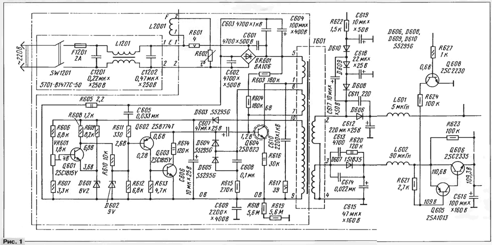
(click to enlarge)
Transistor Q604 has a blocking generator - positive feedback voltage is removed from the winding 7 - 8 of the transformer. The duration of the pulses generated by the blocking generator, i.e., the time of the transistor Q604 in the saturated state, is determined by the operation of the pulse width modulator (PWM).
The capacitor C607 is connected to the base of the transistor Q604, which during the closed state of the transistor is charged by a voltage pulse of the winding 7 - 8 of the transformer through the diode D604. When the Q602, Q603 PWM transistors are opened, the capacitor C607 is connected to the emitter junction of the saturated transistor Q604, and the discharge current of the capacitor, flowing through the transistors and the resistor R616, quickly closes the transistor Q604. The bias voltage to the base of transistor Q604 is supplied through resistors R603, R604. The C610R617 circuit limits pulses to the collector of the transistor Q604, protecting it from breakdown.
To power the DC amplifier on the transistor Q601, the AC voltage from the winding 9 - 10 is rectified by the diode D603 and charges the capacitor C606. The voltage at the emitter of the transistor Q601 is stabilized by the parametric stabilizer on the elements D601, R609, and the voltage to the base of the transistor is removed from the measuring resistor divider R606VR601R607. The latter depends on the voltage on the winding 9 - 10 of the transformer, i.e. the output voltage levels of the power supply unit + 110 and +12 V. The voltage across the resistor R608 - the collector load of the transistor Q601 serves as the error voltage and controls the moment of PWM opening on transistors Q602, Q603. The tuning resistor VR601 sets the output voltage + 110 V.
From the resistor R605 through the chain C605R611 the sawtooth voltage is removed to the base of the PWM driver O602. It also receives error voltage from the collector of transistor Q601. Depending on the last PWM it is opened sooner or later, counting from the moment of opening of the transistor Q604. Transistors Q602, Q603 are an analog of the trinistor. The principle of its operation is analogous to the operation of the trinistor in the pulsed power module MPZ-3.
With increasing network voltage or decreasing the load, the voltage on the winding 9 - 10 of the T601 transformer increases. As a result, the transistors Q602, Q603 open earlier, closing the output transistor Q604 at an earlier time. This reduces the energy stored in the transformer T601, which compensates for the increase in the mains voltage.
When the voltage of the network decreases, the voltage on the winding 9-10 of the transformer T601 will be lower, respectively. At the collector of the transistor Q601, the error voltage decreases, the PWM opens at a later time, and the amount of energy transferred to the secondary circuit increases, compensating for the decrease in the mains voltage.
The secondary rectifiers of the block are made in a half-wave circuit. The winding of 4 to 2 transformers and the elements D606, C612, L601 form a +12 V voltage source used for operation of the remote control system and other low-current circuits. The winding 4 - 3 and the elements D607, L602 enter the voltage source +110 V supplying the output stage of the horizontal scan.
Transistors Q608, Q606, Q605 assembled the power on / off node of the output stage of the horizontal scan. In this way, the TV is turned on or off by the remote control system, ie, it is transferred to the operating or standby mode. In standby mode, the transistor Q606 is closed and the voltage of +110 V is not fed to the output stage of the horizontal scan. In some TV models, relays are used for this purpose.
The typical malfunctions of this power supply unit are similar to those of the module MP3-3. For repair, the board of the unit is removed from the TV cabinet and placed so that there is free access to the elements. In parallel, the capacitor C604 is connected with a resistor of 220 kΩ and a dissipation power of 0.5 W. Through it, the capacitor will be discharged after turning off the TV. One of the pins of each of the elements L601, L602, D608, C617 is soldered out. In this case, the TV's load circuits will be completely disconnected from the power supply. In parallel, the C615 capacitor is connected to an incandescent lamp of 220 V and 25 W, which will serve as the equivalent of the power unit's load.
After repair, before connecting the power supply unit to the TV circuit, it is necessary to check the output transistor of the horizontal scan and the secondary circuits of the line transformer. From the secondary windings of the latter, the voltage is often taken, straightened and smoothed to power the TV units. One of the reasons for the failure of the power supply can be precisely these circuits.
When selecting transistors in order to replace the failed ones, one should be guided by their characteristics indicated in Table. 1.
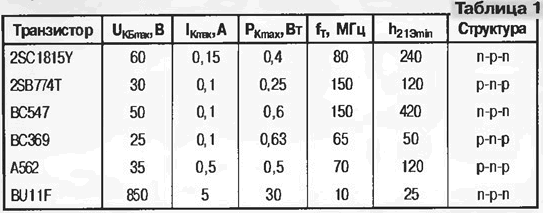
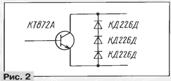
Transistors 2SC1815Y can be replaced by KT3102B, 2SB774T - on KT3107B, and 2SD820, BU11F - on KT872A. The latter is attached to the heat sink with an insulating spacer. Diodes can be replaced by KD209B, KD226A, KD226B.
The output transistors of the horizontal scan 2SD2333, 2SD1876, 2SD1877, 2SD1554 and others having an integrated damper diode are replaced with KT872A as shown in Fig. 2. Attach it to the heat sink through an insulating spacer. You can use and transistors KT846V, KT838A, but there will be difficulties with their attachment to the heat sink.
If the selector of the channels of the imported TV fails, a replacement for the selectors SK-M-24 and SK-D-24 is possible. The correspondence of their conclusions, for example, to the conclusions of the selector TUGZ1-C07 is shown in Table. 2.
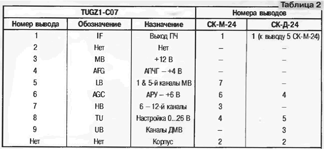
The letters of the selector outputs are found on the TV board, and the pin numbers on the selector housing. Inside the TV, domestic selectors are fixed in any way and output the antenna jacks to the TV cabinet. All connections (wiring) are made, if possible, by short conductors.
In the extreme case, if it is impossible to repair the switching power supply of an imported TV, it can be recommended to replace it with domestic MPZ-3, MP-42 or others. It is possible that the unit is fully suitable for replacement, depending on the brand of the imported TV. If the output voltages do not correspond to those used in the TV, you will have to switch the secondary windings of the pulse transformer as needed and adjust the sources to the corresponding voltage for the TV. The unit is loaded with an incandescent lamp of 40 W and 220 V when connected to a winding with a voltage of 130 ... 150 V.
It should be remembered that on unloaded windings in idle mode there will be a little overestimated voltage. Unused windings are left unconnected. Do not forget to also connect the demagnetize loop.
The switching power supply unit is placed on an empty place inside the TV and securely fixed.
See more articles section.
The voltage drop is not as terrible as it might seem at first glance. Yes, it can lead to malfunctions, causes breakdown of TV units. But all this is just one of the problems that can happen with the technique for the home. To solve this problem, it is necessary to repair the power supply of the TV, independently or by calling the master - it's up to you. Of course, council number 1 in such cases - to call an experienced tele-master. This saves time, preserves the integrity of the nervous system, and also does not significantly affect the purse, because the repair of TV is now inexpensive. But if the user has a strong desire to personally carry out all the work, this article will be very useful.
TV Power Supply Repair Manual
1) Check the health of the unit. To do this, turn on the TV, check the indicator of the standby mode for activity. If it burns, there is a high probability that the problem is not in the power supply.
2) Turn off the TV and remove the case. Our primary goal is to check the scheme. The check is carried out by searching for the fragments of the circuit of defects of contacts, damages, blown capacitors, damaged resistors. If contact damage is detected, they should be replaced with a soldering iron to prevent damage. If the circuit is broken, it will most likely have to be replaced with a new one. If the capacitors are swollen, they must be replaced by workers. Checking the resistors involves replacing the non-working with regularly functioning ones.
3) It is necessary to check the entire power circuit of the TV from the beginning, and to the final point. Our goal is to first call the power cord. After that, check the fuse, then the power switch (if available). The final point is to check the rectifier bridge, after we were convinced that the chokes in the power circuit are working properly.
4) The most thorough check - the diodes and transistors, carried out at the end. Soldering of a part for diagnostics is made only when there is a certainty of its malfunction, or if there are signs of defects.
5) It is also important to check the short circuit in secondary power circuits. It is carried out by checking the outputs of the capacitors for the presence of a short circuit.
Only after troubleshooting, found by checking each item, can you check the operation of the TV under current. Repairing the power supply of the TV, especially if it's done incorrectly, can only exacerbate the situation. Therefore, if the owner does not have confidence in the corrected condition of the BP, it is better not to take risks. Call the telemaster at home, he quickly fix it, find the cause of the malfunction. Moreover, when it turns out that the unit is hopelessly burnt, and the only way to repair it is to replace it completely, you will need to search for the necessary details. It is better to immediately turn to a specialist who not only conducts diagnostics professionally, but also brings the necessary components to the TV at a low price.
In this article we will consider malfunction of power supply unit CRT TV .
CRT TV (cathode ray tube) is a device for receiving and displaying information along with audio. It consists of a channel selector, detectors and amplifiers of radio / video signal, frame and line scanning units, decoding unit, RGB amplifier, cathode ray tube and power supply unit.
Typical power supply failure CRT (CRT) of TVs
Failure tV power supply mainly due to jumps in the power grid, poor quality or aging of individual components. The following are typical faults of several TV models.
SONY KV-M1431K (BE-2A) / RM694
Power Supply This TV generates a secondary, stabilized voltage necessary for the operation of individual units. The converter is built on a PWM controller TR54041.
Typical problems and malfunctions:
The stabilizer + 5V does not work or is faulty. It is necessary to measure the 5th pin IC004 to + 5V, if not, then replace it.
Does not work + 8V. Similarly measure C614, in the absence of voltage, test R613 for an open. Elements D606, C614 and winding 2-12 T601.
Low tone from T601. Most likely an overload of the secondary channel. It is necessary to find an overloaded channel with an ohmmeter and eliminate the cause.
There are no output voltages of the PSU. Here, either the mains power supply circuit is broken or the converter is faulty. First, you need to measure 80V on the IC601 (3rd output). In the absence of voltage, ring the chain: F601-S601-T605-R601-D601-winding 3-7 T601-IC601 (3rd output). Also check for short circuit 11-13, 13-15 T601, circuit C607, R614, R606, D607, C618, R602, R611. If everything is correct, then replace IC601.
The fuse F601 blows. First of all, it is necessary to check the input elements (indicated on the diagram) with an ohmmeter, namely: a mains filter, demagnetization system, rectifier. If during the test it turned out that all the elements are in good order, then we have to drop IC601 and call 2,3,4 conclusions. If there is a short circuit, then also check the winding 3-7 T601, C603, C606, Q601, R609, R615 (protection), R602, R611 (start circuit).