THEME 4. BIPOLAR TRANSISTORS
4.1 Design and principle of operation
A bipolar transistor is a semiconductor device consisting of three areas with alternating types of electrical conductivity and suitable for power amplification.
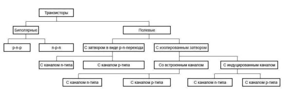
Currently released bipolar transistors can be classified by the following features:
According to the material: germanium and silicon;
By type of conduction areas: type pnp and npn;
By power: small (Rmah £ 0.3W), medium (Rmah £ 1.5W) and high power (Rmah\u003e 1.5W);
By frequency: low-frequency, mid-frequency, high-frequency and microwave.
In bipolar transistors, the current is determined by the movement of charge carriers of two types: electrons and holes (or main and minor). Hence their name is bipolar.
Currently, only transistors with planar pn-junctions are manufactured and used.
The device of a planar bipolar transistor is shown schematically in Fig. 4.1.
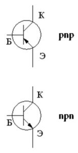
It is a plate of germanium or silicon, in which three regions with different electrical conductivities are created. At the transistor type nn the middle region has a hole, and the outermost regions have electronic conductivity.
Transistors of p-n-p type have a middle area with electronic, and extreme areas with hole electrical conductivity.
The middle region of the transistor is called the base, one extreme region - the emitter, the other - the collector. Thus, in the transistor there are two pn-transitions: emitter - between the emitter and the base and collector - between the base and the collector. The emitter junction area is smaller than the collector junction area.
An emitter is a transistor area whose purpose is to inject charge carriers into the base. Collector is the area, the purpose of which is the extraction of charge carriers from the base. The base is the area into which the emitters are injected into charge carriers that are non-essential for this area.
The concentration of the main charge carriers in the emitter is many times greater than the concentration of the main charge carriers in the base, and their concentration in the collector is somewhat lower than the concentration in the emitter. Therefore, the emitter conductivity is several orders of magnitude higher than the base conductivity, and the collector conductivity is slightly less than the emitter conductivity.
Conclusions are made from the base, emitter and collector. Depending on which of the conclusions is common to the input and output circuits, there are three switching circuits for the transistor: with a common base (ON), common emitter (OE), common collector (OK).
The input, or control, circuit serves to control the operation of the transistor. In the output, or controlled, the chain obtained increased oscillations. The source of amplified vibrations is included in the input circuit, and the load is included in the output circuit.
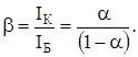
Consider the principle of operation of the transistor on the example transistor pnp –Type included in the scheme with a common base (Fig. 4.2).
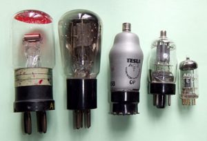
Figure 4.2 - The principle of operation of a bipolar transistor (pnp type)
The external voltages of the two power sources EE and Ek are connected to the transistor in such a way that the emitter junction P1 is displaced in the forward direction (forward voltage) and the collector junction P2 - in the reverse direction (reverse voltage).
If a reverse voltage is applied to the collector junction, and the emitter circuit is open, then a small reverse current Iko (units of microamps) flows into the collector circuit. This current arises under the action of reverse voltage and is created by the directional movement of minority charge carriers of the base holes and collector electrons through the collector junction. The reverse current flows through the circuit: + Ek, base-collector, –Ek. The magnitude of the reverse collector current does not depend on the voltage on the collector, but depends on the temperature of the semiconductor.
When a direct voltage ЕE in the forward direction is included in the emitter circuit, the potential barrier of the emitter junction decreases. Injection (injection) of holes into the base begins.
The external voltage applied to the transistor turns out to be applied mainly to the transitions P1 and P2, since they have a high resistance compared to the resistance of the base, emitter and collector areas. Therefore, the holes injected into the base move in it through diffusion. In this case, the holes recombine with the electrons of the base. Since the carrier concentration in the base is significantly lower than in the emitter, very few holes recombine. With a small base thickness, almost all the holes will reach the collector junction P2. In place of the recombined electrons, electrons enter the base from the EC power source. Holes, recombined with electrons in the base, create a current base IB.
Under the action of the reverse voltage Ek, the potential barrier of the collector junction increases, the thickness of the junction P2 increases. But the potential barrier of the collector junction does not create obstacles for holes to pass through it. The holes that enter the collector junction region enter a strong accelerating field created at the junction by a collector voltage, and are extracted (pulled in) by the collector, creating a collector current Ik. Collector current flows through the circuit: + Ek, base-collector, -Ek.
Thus, three currents flow in the transistor: the emitter current, the collector and the base.
In the wire, which is the output of the base, the currents of the emitter and collector are directed opposite. Consequently, the base current is equal to the difference between the emitter and collector currents: IБ = IЕ - IК.
Physical processes in an n-p-n type transistor proceed similarly to processes in a p-n-p type transistor.
The total emitter current IE is determined by the number of main charge carriers injected by the emitter. The main part of these charge carriers reaching the collector, creates a collector current Ik. An insignificant part of the carriers injected into the base is recombined in the base, creating a base current IB. Consequently, the emitter current is divided into the base and collector currents, i.e. IE = IB + Ik.
The emitter current is the input current and the collector current is the output current. The output current is part of the input, i.e.
(4.1)where a is the current transfer ratio for the circuit ON;
Since the output current is less than the input current, the coefficient a<1. Он показывает, какая часть инжектированных в базу носителей заряда достигает коллектора. Обычно величина a составляет 0,95¸0,995.
In the common emitter circuit, the output current is the collector current, and the input current is the base current. Current Gain for OE Circuit:
(4.2)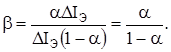 (4.3)
(4.3)
Consequently, the current gain for the OE circuit is tens of units.
The output current of the transistor depends on the input current. Therefore, the transistor is a device controlled by current.
Changes in the emitter current caused by a change in the voltage of the emitter junction are completely transmitted to the collector circuit, causing a change in the collector current. And since the voltage of the source of the collector power Ек is much higher than the emitter Ee, then the power consumed in the collector circuit Рк will be much more than the power in the emitter circuit Рэ. Thus, it is possible to control high power in the collector circuit of the transistor with low power consumed in the emitter circuit, i.e. power gain takes place.
4.2 Circuits for switching bipolar transistors
In the electrical circuit, the transistor is included in such a way that one of its terminals (electrode) is input, the second output, and the third common to the input and output circuits. Depending on which electrode is common, there are three switching circuits for switching on the transistors: ON, MA and OK. These circuits for the pnp transistor are shown in fig. 4.3. For the n-p-n transistor, only the polarities of the voltages and the direction of the currents change in the switching circuits. In any switching circuit of the transistor (in active mode), the polarity of switching on the power supply must be chosen so that the emitter junction is turned on in the forward direction and the collector junction in the opposite direction.
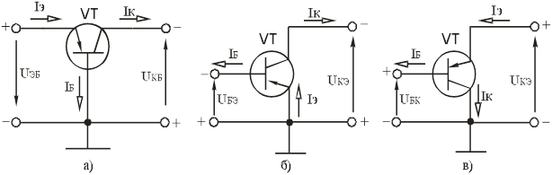
Figure 4.3 - Circuits for switching on bipolar transistors: a) ON; b) OE; c) OK
4.3 Static characteristics of bipolar transistors
The static mode of operation of the transistor is called the mode when there is no load in the output circuit.
Static characteristics of transistors are called graphically expressed dependences of voltage and current of the input circuit (input VAC) and output circuit (output VAC). The type of characteristics depends on how the transistor is turned on.
4.3.1 Characteristics of the transistor included in the OB scheme
IE = f (UEB) with UKB = const (Fig. 4.4, a).
IК = f (UКБ) with IЕ = const (Fig. 4.4, b).
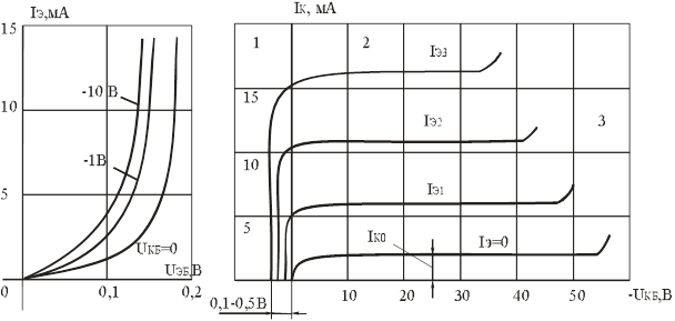
Figure 4.4 - Static characteristics of a bipolar transistor included in the OB scheme
The output current – voltage characteristics have three characteristic regions: 1 — strong dependence of Ik on UKB (nonlinear initial region); 2 - weak dependence of Ik on UKB (linear region); 3 - breakdown of the collector junction.
A feature of characteristics in area 2 is their slight rise with increasing voltage UKB.
4.3.2 Characteristics of the transistor included in the OE scheme:
The input characteristic is the dependency:
IB = f (UБЭ) with UКЭ = const (Fig. 4.5, b).
The output characteristic is the dependency:
IК = f (UКЭ) at IБ = const (fig. 4.5, a).
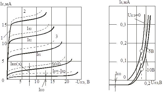
Figure 4.5 - Static characteristics of a bipolar transistor connected according to the OE scheme
The transistor in the OE circuit provides current gain. Current gain in the OE circuit:
 If the coefficient a for transistors is a = 0.9¸0.99, then the coefficient b = 9¸99. This is the most important advantage of switching on the transistor according to the OE scheme, which, in particular, determines the wider practical application of this switching circuit in comparison with the OT circuit.
 From the principle of operation of the transistor, it is known that two components of the current flow in the opposite direction through the output of the base (Fig. 4.6): the reverse current of the collector junction ICO and part of the emitter current (1 - a) IE. In this regard, the zero value of the base current (IB = 0) is determined by the equality of the indicated component currents, i.e. (1 - a) IE = IKO. The zero input current corresponds to the emitter current IE = IKO / (1 − a) = (1 + b) IKO and collector current
. In other words, at zero base current (IB = 0), a current flows through the transistor in the OE circuit, called the initial or through current ICO (E) and equal to (1+ b) IKO.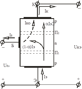
Figure 4.6 - the circuit of the transistor with a common emitter (circuit OE)
4.4 Basic parameters
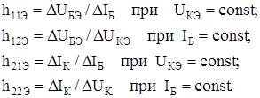
For the analysis and calculation of circuits with bipolar transistors use the so-called h - parameters of the transistor, connected according to the OE scheme.
The electrical state of the transistor included in the OE scheme is characterized by the values IB, IBE, IK, UKE.
The system h - parameters include the following values:
1. Input resistance
h11 = DU1 / DI1 with U2 = const. (4.4)
is the resistance of the transistor to an alternating input current at which a short circuit at the output, i.e. in the absence of output AC voltage.
2. Voltage feedback ratio:
h12 = DU1 / DU2 when I1 = const. (4.5)
shows how much of the input AC voltage is transmitted to the input of the transistor due to the feedback in it.
3. Force current coefficient (current transfer ratio):
h21 = DI2 / DI1 when U2 = const. (4.6)
shows the ac gain by the transistor in the no-load mode.
4. Output Conductivity:
h22 = DI2 / DU2 with I1 = const. (4.7)
represents the conductivity for alternating current between the output terminals of the transistor.
Output impedance Rout = 1 / h22.
For a common emitter circuit, the following equations are true:
 (4.8)
(4.8)
To prevent overheating of the collector junction, it is necessary that the power released in it during the passage of the collector current does not exceed a certain maximum value:
In addition, there are limitations on the collector voltage:
and collector current:
4.5 Modes of operation of bipolar transistors
The transistor can operate in three modes, depending on the voltage at its transitions. When operating in active mode, the voltage is direct at the emitter junction, and the reverse at the collector one.
The cut-off mode, or locking, is achieved by applying a reverse voltage to both transitions (both pn-transitions are closed).
If, on both transitions, the voltage is direct (both pn-junctions are open), then the transistor operates in the saturation mode.
In the cutoff mode and saturation mode, the transistor control is almost absent. In the active mode, such control is carried out most efficiently, and the transistor can perform the functions of the active element of an electrical circuit (amplification, generation, etc.).
4.6 Scope
Bipolar transistors are semiconductor devices for universal use and are widely used in various amplifiers, oscillators, pulsed and key devices.
4.7 The simplest amplifying cascade on a bipolar transistor
The application of the transistor according to the scheme with a common emitter is most widely used (Fig. 4.7)
The main elements of the circuit are the EC power supply, the controlled element —VT transistor and resistor Rc. These elements form the main (output) circuit of the amplifying stage, in which due to the flow of the controlled current an amplified alternating voltage is created at the output of the circuit.
The remaining elements perform a supporting role. The capacitor Cp is separable. In the absence of this capacitor in the circuit of the input source would create a constant current from the power source Ek.
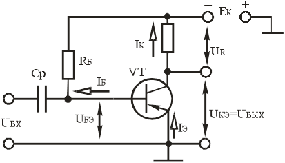
Figure 4.7 - Scheme of the simplest amplifier stage on a bipolar transistor according to the circuit with a common emitter
The resistor RB, included in the base circuit, ensures that the transistor operates in the rest mode, i.e. in the absence of an input signal. The rest mode is provided by the current of the base of rest IB "Ek / RB.
With the help of the resistor Rk, the output voltage is generated, i.e. Rк performs the function of creating a varying voltage in the output circuit due to the flow in it of a current controlled through the base circuit.
For the collector circuit of the amplifier stage, we can write the following equation of the electric state:
Ek = Uke + IkRk, (4.10)
ie, the sum of the voltage drop across the resistor Rk and the collector-emitter voltage Uke of the transistor is always equal to a constant value - the emf of the power source Ek.
The amplification process is based on the conversion of the energy of the dc voltage source ek to the ac voltage in the output circuit due to the change in the resistance of the controlled element (transistor) according to the law specified by the input signal.
When an ac voltage voltage uin is applied to the input of the amplifier circuit, a variable component of current IB is created in the base transistor circuit, which means the base current will change. A change in the base current leads to a change in the value of the collector current (IK = bIB), and therefore to a change in the values of voltages on the resistance Rk and Uke. Amplifying abilities are due to the fact that the change in the values of the collector current is b times greater than the base current.
4.8 Calculation of electrical circuits with bipolar transistors
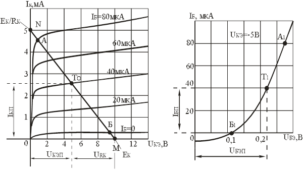
For the collector circuit of the amplifier cascade (Fig. 4.7), in accordance with the second Kirchhoff law, equation (4.10) is valid.
Volt-ampere characteristic of collector resistor RК is linear, and volt-ampere characteristics of the transistor are non-linear collector characteristics of the transistor (Fig. 4.5, a), connected according to the OE scheme.
The calculation of such a nonlinear circuit, that is, the determination of IK, URK and UKE for various values of base current IB and resistors RK can be drawn graphically. To do this, on the family of collector characteristics (Fig. 4.5, a) it is necessary to draw from the point EK on the abscissa axis the volt-ampere characteristic of the resistor RК, which satisfies the equation:
Uke = Ek - RkIk. (4.11)
This characteristic is built on two points:
Uke = Ek when Ik = 0 on the x-axis and Ik = Ek / Rk when Uke = 0 on the ordinate axis. Thus constructed, the IVC of the collector resistor RK is called the load line. The points of its intersection with the collector characteristics give a graphic solution of equation (4.11) for a given resistance Rk and various values of base current IB. From these points you can determine the collector current Ik, which is the same for a transistor and a resistor Rc, as well as the voltage UKE and URK.
The point of intersection of the load line with one of the static IV characteristics is called the working point of the transistor. Changing IB, you can move it along the load line. The initial position of this point in the absence of an input variable signal is called the point of rest - T0.
 a) b)
a) b) Figure 4.8 - Graph-analytical calculation of the operating mode of the transistor using the output and input characteristics.
The rest point (operating point) T0 determines the current IKP and the voltage UKEP in the rest mode. By these values, you can find the power of the RCP, which is released in the transistor in the rest mode, which should not exceed the maximum power of the RK max, which is one of the parameters of the transistor:
PSC = IKP × UKEP £ RK max. (4.12)
Reference books usually do not give a family of input characteristics, but give only characteristics for UKE = 0 and for some UKE\u003e 0.
Input characteristics for different UKE, exceeding 1B, are located very close to each other. Therefore, the calculation of input currents and voltages can be approximated by the input characteristic for UKE\u003e 0, taken from the directory.
The points A, To and B of the output working characteristic are transferred to this curve, and the points A1, T1 and B1 are obtained (Fig. 4.8 b). Operating point T1 determines constant pressure base UBEP and direct current IBP base.
The resistance of the resistor RB (ensures the operation of the transistor in the quiescent mode), through which a constant voltage is applied to the base from the EC source:
 (4.13)
In the active (amplification) mode, the point of rest of the transistor That is approximately in the middle of the section of the load line AB, and the operating point does not extend beyond the limits of the section AB.
Semiconductor triodes are used to amplify electrical impulses. Since the transistor works by changing the voltage in the network, it can regulate the strength of the current in a particular electrical device.
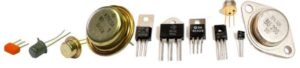
Kinds of transistors
A transistor is a semiconductor active radio element that is needed to generate, transform and amplify an electrical signal (its frequency and strength). It is also called the semiconductor triode. This element of the scheme is necessary for the work of almost all known electrical devices (ignition switch, diode bridgepower supply, load switch, sensor, etc.). It was patented at the beginning of the 20th century with the participation of the famous physicist Julius Edgar Lilienfeld, but his improvement took place only on the basis of the already existing bipolar in the 60s. Only 20 years later Shockley, Bardin and Brattein created the first bipolar triodes.
Photo - design
Structurally, the transistor consists of three electrodes: a base, an emitter, a collector. Here, the emitter and collector represent the main parts of the device, the base performs the functions of network control, current amplification and conversion. The circuit with this electric element is denoted as three electrode taps enclosed in a circle. The arrow indicates the direction of the current in the emitter.
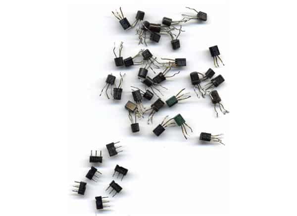
Photo - types of triodes
There are two types of transistors: field and bipolar, they differ from each other by the principle of operation and the area of use. The field element is controlled by the incoming mains voltage, while the bipolar is controlled by the current. Consider their work in more detail.
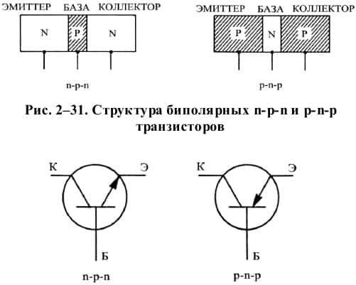
Photo - structure
A field-effect transistor is a single junction element, since a charge with only one sign (+ or -) flows through it. Therefore, they are called unipolar. These details are classified by type of control:
- With pn junction or Schottky barrier;
- With isolated shutter MOSFET;
- MDP or metal-dielectric conductor.
An isolated element is practically no different from a non-insulated, with the exception of an additional dielectric layer between the gate and the channel. It is called the MOSFET because of the design: metal oxide semiconductor.
Photo - field device
A bipolar transistor is known for its ability to pass charges with a different sign through a single base. In this element, the current moves through the base to the collector. There are such performances:
- npn;
- pnp;
- With isolated IGBT tap.
npn are reverse transistors. pnp - with a straight line. One of the subspecies of the reverse semiconductor triode is an optotron, which opens, not by current, but by recognition of light. The element in this mode of operation is used in different light sensors, switches, etc.
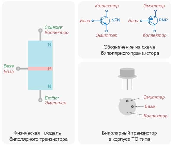
Photo - Bipolar device
In addition, these elements can vary in power, size, material used for the base. The power of transistors ranges from 100 mW to 1 W and more, modern electronics uses all kinds, depending on the purpose and design features device.
Previously, bipolar transistors had a relatively large size, compared with modern parts. Now electronics even uses so-called “islands” - these are elements that are represented in the diagram as a dot. They are practically imperceptible to the prying eye, but allow strong impulses to be passed and controlled.
Each type of transistor has certain advantages and disadvantages:
- Field can be destroyed at low temperatures and high humidity;
- The field signal controller is very sensitive to static electricity. Given that current discharges of up to several thousand volts pass through the amplifier, its gate can be easily destroyed;
- Bipolar models have little resistance;
- The electronic circuit with a common base for connecting the reverse transistors must be connected to two different power sources.
The principle of operation for beginners
The field triode is controlled by exposure to current carriers electric fieldand not the current input base circuit. The basis of this element is a silicon-phosphorus plate of type n, which differs from a mixture of silicon and boron by a large number of free electrodes. On this plate is a gate with a channel - it is called the p-region. This channel has two ends - the drain and the source, which also have a region p, but only with an increased number of electrons. Due to this, a pn junction is created between the channel and the gate.
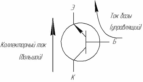
Photo - the principle of work
Contact pins interconnect the gate, source and drain. If a plus is connected to the source and a minus from the power supply to the drain, then the channel system will begin to receive current. It will be created by the movement of electrons between the conductors of the circuit. This is called the drain current. Note that when a positive terminal is connected to the source, the depletion region expands and the channel narrows, thereby dramatically increasing the flow resistance. Accordingly, if the area of depletion will narrow, then the drain current will increase. This is how a field effect transistor works.
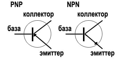
Photo - the difference between triodes
Bipolar reverse npn works due to the emitter-collector circuit. When the current is connected to the circuit, the transistor opens. If you change the voltage supplied to the base, it will be possible to control the current in the circuit. This principle of operation is used in most models of modern electronics.
Mainly electrical engineering uses polar and unipolar type transistors to amplify the signals of various sensors or control the current of the power supply network. A remarkable feature of these elements is that they can be used to assemble various logical microcircuits acting as a logical multiplier, a negative, etc.
Video: Transistor Explained
https://www.youtube.com/watch?v=37V3gDGvhPQ
Work in the scheme
Transistors are one of the most popular and necessary circuit elements in electronics. Consider how these elements are used on the trigger and regenerator. The Schmitt trigger pulse is a generator in which all the incoming voltage is divided by a comparator into three ranges. It consists of transistors, which are interconnected by galvanic coupling and a resistor, load resistors and a capacitor.
Photo - the work of the transistor in the Schmitt trigger
When the trigger is connected to a power source, one of its MOSFET opens and the other closes. After this, some voltage appears in the circuit, the level of which depends on the strapping of the circuit elements.
The use of semiconductor triodes in the regenerator is necessary to simplify the regulation of the frequency of the current. The main advantage of using a transistor circuit here is that the resulting cascade can control waves of any size, ranging from ultrasound.
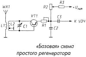
Photo - regenerator circuit
Such a regenerator consists of two 0.5 V bipolar transistors, a coil and a resistor. Such a circuit can be connected as an autogenerator, then most of the coil will go to the collector outlet, and the smaller - to the base. The voltage to the transistors is supplied through resistors, they can be used to change the voltage and resistance of the signal between the emitter and the base.
The original name of the radio component is the triode, according to the number of contacts. This radio element is able to control the current in electrical circuit, under the influence of an external signal. Unique properties are used in amplifiers, generators and other similar circuit solutions.
Designation of transistors on the circuit
For a long time tube triodes reigned in electronics. Inside the sealed flask, in a special gas or vacuum environment, there were three main components of the triode:
- Cathode
- Grid
When a low-power control signal was applied to the grid, incomparably large values could be passed between the cathode and the anode. The magnitude of the working current of the triode is many times higher than that of the manager. This property allows the radio element to perform the role of an amplifier.
Radio tube-based triodes work quite effectively, especially when high power. However, the dimensions do not allow their use in modern compact devices.
Imagine a mobile phone or pocket player, made on such items.
The second problem is catering. For normal operation, the cathode must be strongly heated for electron emission to begin. Heating a coil requires a lot of electricity. Therefore, scientists around the world have always sought to create a more compact device with the same properties.
The first samples appeared in 1928, and in the middle of the last century, a working semiconductor triode, made by bipolar technology, was introduced. For him stuck the name "transistor".
What is a transistor?
Transistor - a semiconductor electrical device with or without a housing, having three contacts for operation and control. The main property is the same as that of the triode - changing the parameters of the current between the working electrodes with the help of a control signal.
Due to the absence of the need to heat up, the transistors spend a negligible amount of energy to ensure their own performance. And the compact dimensions of the working semiconductor crystal, allow the use of radio components in small-sized structures.
Due to the independence of the working environment, the semiconductor crystals can be used both in a separate package and in chips. Included with the remaining radio elements, transistors are grown directly on a single crystal.
The outstanding mechanical properties of a semiconductor have found application in mobile and portable devices. Transistors are insensitive to vibration, sharp blows. They have a good temperature resistance (with a heavy load they use cooling radiators).
Therefore, fairly quickly lamp triodes were replaced by compact, durable and inexpensive transistors.
However, the use of radio tubes is not discontinued. In powerful radio transmitters, generators - tube amplifiers are successfully used. Some features of high-power radio tubes are unattainable (or the implementation is too expensive) for semiconductor devices.
According to the structure of the crystal. The main directions of construction (and therefore, the properties of the part) - two. They are clearly depicted in the illustration:
To understand what a transistor is - you need to know how it works.
In this video, in detail about the structure of the transistor, what it is for and how it works.
Field effect transistors
They work in the same way as vacuum triodes. They have two working leads (drain and source) and a manager (shutter). Electricity flows between drain and source with intensity that depends on the control signal. A signal in the form of a transverse electric field is formed between the gate and the drain, or the gate and the source.
All varieties of field effect transistors in the illustration:
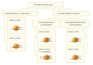
Consider the main types:
Managing pn transition.
The drain and source are connected to a semiconductor wafer. It may be of the n or p type. The control electrode is connected to the plate at help pn transition. The control signal of low power opens the pn channel, forcing the transistor to operate in the signal amplification mode.
The termination of the control signal leads to the disconnection of the channel. Of course, there is a linear relationship between the control signal and the operating current.
The main feature of the field-effect transistor is that the control is carried out not by current, but by voltage. The use of field-effect transistors is mainly integrated circuits. Scanty (close to zero) power consumption allows the use of radio components in systems with compact and low-power power sources, for example, a wrist watch.
High power field-effect transistors are used in high-quality sound amplifiers, as an alternative to vacuum triodes.
Of course, like any other detail - field workers can fail. So as not to throw out a working part by mistake, you can check the transistor at home
How to call a field-effect transistor with a multimeter?
Attention! If your device has the function of checking transistors - use it. We consider a multimeter without such a function.
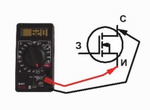
- We transfer the tester to the diode check mode. For the virtual diode, the transition between the drain and the source is taken. A healthy transition works exactly like a semiconductor diode;
- We connect the positive contact of the measuring wire with the source, negative with the drain. If the transistor is good, it should be within 500-600;
- To check the final, you must check the flow of current in the opposite direction. Change the polarity of the connection. The tester shows conditionally infinite resistance. The number 1 on the display.
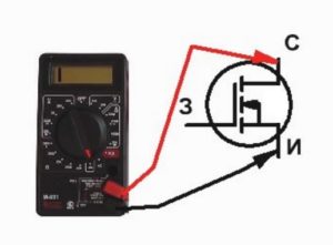
- The field-effect transistor check is not limited to conduction transition testing. It is necessary to check the opening of the working channel. There is no need for a special power source; we are considering how to test a transistor with a multimeter autonomously. Enough power tester to open the transition. Negative probe connect to the source, positive to the control gate. A working transistor will open the source-drain channel.
- A transistor dial in the source-drain channel will show the voltage drop across the p-n junction channel.
- Change the polarity on the source-drain electrodes. If the transistor is normal, the p-n junction channel will close. Check the current in the source-drain channel - a transistor check with a multimeter shows closed pn transition.
MOS transistor with insulated gate.
Unlike the previous model - the gate is separated from the channel by a dielectric. The so-called shutter release occurs only when a certain voltage and a given polarity is reached.
These transistors have a narrow specialization, and are used mainly in the composition of the chip. The technique of how to check the field effect transistor is not suitable here. Actually, this is not necessary, transistors are almost never used.
To fix the read, watch the video on the topic: How to check the field-effect transistor with a multimeter.
Bipolar transistors
The method of operation is fundamentally different from field semiconductor triodes. Two pn junctions are created on a semiconductor chip.
The working current is formed due to charge transfer either by electrons or by so-called holes. That is, the current can flow in any (but only one) direction. Therefore, transistors of this type are called bipolar.
The bipolar transistor, like any other, has three outputs.
- Base. Connects with the middle layer of semiconductor;
- Emitter and collector. These contacts have a connection with the outer layers of the crystal.
Due to the versatility of the work, a lot of schemes are performed on the bipolar stations - mainly amplifying ones.
- Scheme with a common base. Universally connected. The sparing mode, but at the same time the ability to amplify the working signal is weak;
- Scheme with a common emitter. Very high efficiency, the working signal is amplified with the highest possible coefficient. Disadvantages - complex calculation of the input resistance (when designing circuits) and a strong dependence on temperature;
- Scheme with a common collector. In comparison with the previous inclusion option, the signal amplification ability is significantly less. You can effectively use the input resistance of the element.
Modes of operation of transistors made by bipolar technology:
Active mode is direct.
Emitter base in the open state, the collector base is closed. How to check the transistor with a multimeter in this mode? Knowing the wiring diagram - like a normal diode.
Active inversion mode.
The emitter base is closed, the collector base is open. The verification of the radio element is carried out in a similar way, only the polarity of the tester is reversed.
Saturation.
Transitions are in the open state. The launch of this mode is carried out by simultaneously connecting to the external source of both transitions. Stable condition.
Cut-off.
Collector junction is included in the inverse direction. The emitter transition works in two directions. Important! To ensure the mode can not be energized above the threshold.
Barrier.
The base is connected to the collector. For soft work in series with the working circuit connects a resistor. The circuit can be used as a diode with a resistive current limiter.
If you understand the principle of operation, questions about how to ring the transistor should not arise. From the point of view of a multimeter, a transistor is a set of diodes. If it is understood in which direction pn junctions are open, the check is reduced to the dialing of virtual diodes.
Watch a detailed video about bipolar transistors, their structure and applications in electronics.
Consider the inclusion of a transistor with a common emitter.
- the very term of the name of this inclusion already speaks about the specifics of this scheme. Common emitter and in Kratz it is OE, implies the fact that the input of this circuit and the output have a common emitter.
Consider the scheme:
In this circuit we see two power sources, the first 1.5 volts, used as an input signal for the transistor and the whole circuit. The second power source is 4.5 volts, its role is the power of the transistor, and the whole circuit. The circuit element Rн is the load of the transistor or, more simply, the consumer.
Now let's follow the work of this circuit itself: the power source of 1.5 volts serves as an input signal for the transistor, acting on the base of the transistor, it opens it. If we consider the full cycle of the base current, it will be like this: the current passes from plus to minus, that is, coming from a 1.5 volt power source, namely from the terminal + the current passes through the common emitter passing through the base and closes its circuit on the battery terminal 1.5 volts At the time of passage of the current through the base of the transistor is open, thereby the transistor allows the second 4.5 volt power source to power RL. Let's see the current flow from the second 4.5 volt power supply. When the transistor is opened by the base input current, a 4.5 volt power source leaves the emitter of the transistor and leaves the collector directly to the load RL.
The gain is equal to the ratio of the collector current to the base current and can usually reach from tens to several hundreds. A transistor connected in a circuit with a common emitter can theoretically give the maximum signal gain in power, relative to other options for switching on the transistor.
Now consider the switching circuit of the transistor with a common collector: 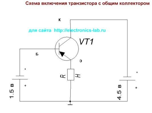
In this scheme, we see that there is a common collector for the input and output of the transistor. Therefore, this circuit is called OK with a common collector.
Consider her work: as in the previous scheme, the input signal to the base, (in our case, this is the base current) opens the transistor. When opening the transistor, the current from the battery 4.5 V passes from the battery terminal + through the load RL to the emitter of the transistor passes through the collector and ends its circle. The input of the cascade with this switch on OK has a high resistance, usually from tenths of a megaoma to several megaohms due to the fact that the collector junction of the transistor is locked. And the output impedance of the cascade, on the contrary, is small, which makes it possible to use such cascades for matching the preceding cascade with the load. A cascade with a transistor connected in a circuit with a common collector does not increase the voltage, but it amplifies the current (usually 10 ... 100 times). We will return to these details in the following articles, since it is not possible to cover everything and everyone at once.
Consider the switching circuit of a common base transistor. 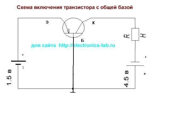
The name ABOUT it already tells us a lot now - it means that the common base for turning on the transistor is relative to the input and output of the transistor.
In this scheme, the input signal is supplied between the base and the emitter - which is what a 1.5-volt battery serves us; The input resistance of the cascade is small and usually lies in the range from units to hundreds of ohms, which is attributed to the lack of the described switching on of the transistor. In addition, for the operation of the cascade with a transistor connected according to the scheme with a common base, two separate power sources are needed, and the gain of the cascade in current is less than one. The gain of the cascade voltage often reaches from tens to several hundred times.
Here are three schemes of switching on the transistor, to expand the knowledge I can add the following:
The higher the frequency of the signal at the input of the transistor stage, the lower the current gain.
The collector junction transistor has a high resistance. Increasing the frequency leads to a decrease in the reactive capacity of the collector junction, which leads to its substantial shunting and deterioration of the amplifying properties of the cascade.