Wiring transistor with a common emitter (OE). In the study of properties, a switching circuit of a transistor with a common emitter is usually used, that is, when the emitter is connected to ground, the collector is connected to the power supply through the load resistance, and the bias voltage is applied to the base. Let's assemble the scheme shown in the picture:
The circuit uses a transistor npn structures, load resistance - 1 kOhm, power source with a voltage of 12 volts and ammeter.
We see that the ammeter shows a very low value of the current flowing through the load resistance and the collector-emitter junction of the transistor. This current is called the leakage current of the n-p-n junction.
By the definition of a transistor, a small base current controls a large current in the collector-emitter circuit (in the circuit with OE).
To create an amplifier stage according to the scheme with OE, one should create an initial base current, such that the transistor is in the operating mode. In our circuit, the transistor is in cut-off mode (the resistance K - E tends to infinity). The second extreme mode is called the saturation mode, that is, when the base receives the maximum current, which does not affect the current flowing into chains K-E (collector current). In this case, it is said that the transistor is open and the collector current is determined by the load resistance, and the transition resistance K - E can be taken as 0. Between these two points, in the middle is the operating current (operating point) of the transistor base.
In practice, to determine the operating mode of the transistor, they measure not the current, but the voltage on the base and on plot K-E. The inclusion of a voltmeter does not require breaking the circuit.
To determine the operating point, you should assemble the circuit shown in the figure:
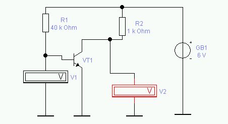
Through the resistor R1 the bias voltage is applied, which creates a base current. Resistance R1, in the course of the experiment, we will change from 40 to 300 kΩ, with a step of 20 kΩ. With a voltmeter V1 we will measure the voltage of the base - the emitter, and a voltmeter of the V2, the voltage of the collector - the emitter.
The measurement results are best recorded in a table, for example, in Microsoft Excel or Open Office Calc.

According to the measurement results, we will construct a graph for the change in the collector-emitter voltage (CE):

We see that when measuring 1-2-3, the QE voltage practically does not change and is close to 0. This mode is called the saturation mode. In this mode, the amplifier stage will work with strong signal distortion, since only negative signal half-wave will be amplified.
In section 12-13-14, the same graph gradually acquires a linear relationship, and the voltage at the collector remains almost unchanged. In such a mode is called a cut-off mode. In this mode, the signal will be amplified, also with large distortions, since only the positive half-waves of the signal will be amplified. Cascades with cut-off mode are used in digital technology as a key with inversion - the logical element "NOT".
To select the operating point of the transistor as an amplifier, you must calculate the point B on the graph. For this, the base voltage at point A should be added to the base voltage at point C and divided in half (find the arithmetic average. (820 + 793) / 2 = 806.5. We see that the base voltage is 806.5 mV, approximately corresponds to 6 - to the measurement - 807 mV. This voltage is at the base of the transistor and corresponds to the operating point of the cascade with a common emitter.
We connect a generator to the amplifier input, and an oscilloscope to the input and output. The input is connected to channel A, and the output of the amplifier to channel B. For decoupling the amplifier cascade by alternating current at the input of the cascade, install capacitors C1 and C1.
We take the frequency of the generator 1000 Hz (1 kHz), and the amplitude of the signal 10 mV. On the oscilloscope, we set the sweep time of 0.5 milliseconds per division, the sensitivity of channel A - 10 millivolts per division and the sensitivity of channel B - 1 volt per division.
![]()
Next, turn on the power supply of the circuit and turn it off after 2-5 seconds. For easy reading of the oscilloscope readings, the input sine wave should be lowered below the Y axis (with the Y position counter), and the output sine wave should be higher than the Y axis in a similar way. We see that the output signal is inverted relative to the input 180 degrees.
Consider the amplitude values of the input and output signals. The input signal has an amplitude of 10 mV (we set this value on the generator), and the output signal was obtained with an amplitude of 1.5 volts (3 divisions along the Y / 2 axis. One division - 1 volt). The ratio of the output voltage of the signal to the input voltage is called the voltage gain of the transistor in a common emitter circuit. Calculate the gain of our transistor Ku = Uin / Uout = 1.5 / 0.01 = 150. That is, the cascade on the transistor, connected according to the OE scheme, amplifies the input signal 150 times.
For the transistor cascade with OE, the following values are valid:
Ku - from 50 to 1500
Ki (current gain) - 10-20
Kp (power gain) - 1000-10000
Rin (input resistance) - 100 ohm - 10 com
Rout (output impedance) - 100 ohm - 100 com
Cascade with OE is usually used as a nasco and high frequency signal amplifier.
Inclusion scheme bipolar transistor with a common emitter is shown in Figure 5.15:
The characteristics of the transistor in this mode will differ from those in the common base mode. In a transistor connected in a circuit with a common emitter, there is a gain not only in voltage but also in current. Input parameters for the circuit with a common emitter will be the base current I b, and the voltage on the collector U c, and the output characteristics will be the collector current I c and voltage on the emitter U e.
Earlier, when analyzing a bipolar transistor in a common base circuit, the connection between the collector current and the emitter current was obtained in the following form:
In the scheme with a common emitter (in accordance with the first Kirchhoff law).
after regrouping the factors we get:

Fig. 5.15. Wiring transistor with a common emitter
The coefficient α / (1-α) before the factor I b shows how the collector current I c changes with a single change in the base current I b. It is called the current gain of the bipolar transistor in a common emitter circuit. Denote this coefficient by β.
(5.31)Since the value of the transmission coefficient α is close to unity (α\u003e 1). When the values of the transmission coefficient α = 0.98 ÷ 0.99, the gain will lie in the range β = 50 ÷ 100.
Taking into account (5.31), as well as I к0 * = I к0 / (1-α), expression (5.30) can be rewritten as:
where I к0 * = (1 + β) I к0 is the thermal current of a single pn junction, which is much greater than the thermal current of the collector I к0, and the value of r к is defined as r к * = r к / (1 + β).
Differentiating equation (5.32) over the base current I b, we get β = ΔI to / ΔI b. It follows that the gain factor β shows how many times the collector current I K changes when the base current I b changes.
To characterize the value of β as a function of the parameters of a bipolar transistor, recall that the transfer coefficient of the emitter current is defined as α = γ · κ, where. Consequently, ![]() . For the value of β, the following value was obtained: β = α / (1-α). Since w / l
. For the value of β, the following value was obtained: β = α / (1-α). Since w / l  (5.33)
Figure 5.16a shows the current-voltage characteristics of a bipolar transistor connected in a circuit with a common emitter with a base current as a parameter of the curves. Comparing these characteristics with similar characteristics for a bipolar transistor in a circuit with a common base, we can see that they are qualitatively similar.
Let us analyze why small changes in the base current I b cause significant changes in the collector current I k. The value of the coefficient β, which is much larger than one, means that the transfer coefficient α is close to unity. In this case, the collector current is close to the emitter current, and the base current (recombination by physical nature) is substantially less than the collector and emitter current. At a value of α = 0.99 out of 100 holes injected through the emitter junction, 99 are extracted through the collector junction, and only one will recombine with electrons in the base and give a contribution to base current.

Fig. 5.16. Volt-ampere characteristics of a bipolar transistor KT215V, connected according to the scheme with a common emitter:
a) input characteristics; b) output characteristics
A twofold increase in the base current (two holes must recombine) will cause twice as large injection through the emitter junction (200 holes must be injected) and, accordingly, extraction through the collector one (198 holes extracted). Thus, a small change in the base current, for example, from 5 to 10 μA, causes large changes in the collector current, respectively, from 500 μA to 1000 μA.
The circuit for switching on a bipolar transistor with a common emitter is shown in Figure 5.15:
The characteristics of the transistor in this mode will differ from those in the common base mode. In a transistor connected in a circuit with a common emitter, there is a gain not only in voltage but also in current. Input parameters for the circuit with a common emitter will be the base current I b, and the voltage on the collector U c, and the output characteristics will be the collector current I c and voltage on the emitter U e.
Earlier, when analyzing a bipolar transistor in a common base circuit, the connection between the collector current and the emitter current was obtained in the following form:
In the scheme with a common emitter (in accordance with the first Kirchhoff law).
after regrouping the factors we get: ![]() (5.30)
(5.30)

Fig. 5.15. Wiring transistor with a common emitter
The coefficient α / (1-α) before the factor I b shows how the collector current I c changes with a single change in the base current I b. It is called the current gain of the bipolar transistor in a common emitter circuit. Denote this coefficient by β.
Since the value of the transmission coefficient α is close to unity (α< 1), то из уравнения (5.31) следует, что коэффициент усиления β будет существенно больше единицы (β >\u003e 1). When the values of the transmission coefficient α = 0.98 ÷ 0.99, the gain will lie in the range β = 50 ÷ 100.
Taking into account (5.31), as well as I к0 * = I к0 / (1-α), expression (5.30) can be rewritten as:
![]() (5.32)
(5.32)
where I к0 * = (1 + β) I к0 is the thermal current of a single pn junction, which is much greater than the thermal current of the collector I к0, and the value of r к is defined as r к * = r к / (1 + β).
Differentiating equation (5.32) over the base current I b, we get β = ΔI to / ΔI b. It follows that the gain factor β shows how many times the collector current I K changes when the base current I b changes.
To characterize the value of β as a function of the parameters of a bipolar transistor, recall that the transfer coefficient of the emitter current is defined as α = γ · κ, where. Consequently, ![]() . For the value of β, the following value was obtained: β = α / (1-α). Since w / l<< 1, а γ ≈ 1, получаем:
. For the value of β, the following value was obtained: β = α / (1-α). Since w / l<< 1, а γ ≈ 1, получаем:
 (5.33)
Figure 5.16a shows the current-voltage characteristics of a bipolar transistor connected in a circuit with a common emitter with a base current as a parameter of the curves. Comparing these characteristics with similar characteristics for a bipolar transistor in a circuit with a common base, we can see that they are qualitatively similar.
Let us analyze why small changes in the base current I b cause significant changes in the collector current I k. The value of the coefficient β, which is much larger than one, means that the transfer coefficient α is close to unity. In this case, the collector current is close to the emitter current, and the base current (recombination by physical nature) is substantially less than the collector and emitter current. At a value of α = 0.99 out of 100 holes injected through the emitter junction, 99 are extracted through the collector junction, and only one will recombine with electrons in the base and give a contribution to the base current.
Fig. 5.16. The current-voltage characteristics of a bipolar transistor KT215V, connected according to the scheme with a common emitter: a) input characteristics; b) output characteristics
A twofold increase in the base current (two holes must recombine) will cause twice as large injection through the emitter junction (200 holes must be injected) and, accordingly, extraction through the collector one (198 holes extracted). Thus, a small change in the base current, for example, from 5 to 10 μA, causes large changes in the collector current, respectively, from 500 μA to 1000 μA.
The scheme of inclusion of the transistor with a common base
The circuit of the transistor with a common collector
Wiring transistor with a common emitter
Bipolar Transistor Power Circuits
A signal source is connected between the base and the emitter of a transistor connected in accordance with a common emitter circuit, and a load is connected to the collector. To the emitter of the transistor connect the poles of the same signs of power sources. The input current of the cascade is the base current of the transistor, and the output current is the collector current. This is shown in Figure 20, for example, when a bipolar pnp transistor is connected to an electrical circuit.
Figure 20 - Circuit with a common emitter transistor pnp
In practice, they manage with one power source, not two. The direction of current flow at the terminals of the transistor is given in the figure. Turning on the npn transistor is completely analogous to turning on the pnp transistor, but in this case you have to change the polarity of both power supplies.

Figure 21 - Scheme with a common emitter transistor n-p-n
The gain of the cascade is equal to the ratio of the collector current to the base current and can usually reach from tens to several hundreds. A transistor connected in a circuit with a common emitter can theoretically give the maximum signal gain in power, relative to other options for switching on the transistor. The input impedance of the considered cascade, equal to the ratio of the base-emitter voltage to the base current, ranges from hundreds to thousands of ohms. This is less than the cascade with a transistor connected in a circuit with a common collector. The output signal of the cascade with a common emitter has a phase shift of 180 ° relative to the input signal. Temperature fluctuations have a significant impact on the operation mode of a transistor connected in accordance with a common emitter circuit, and therefore special temperature stabilization circuits should be used. Due to the fact that the resistance of the collector junction of the transistor in the considered cascade is higher than in the cascade with a common base, more time is required for the recombination of charge carriers, and, therefore, the cascade with a common emitter has the worst frequency property.
A load is connected to the emitter of a transistor connected in a circuit with a common collector, an input signal is supplied to the base. The input current of the cascade is the base current of the transistor, and the output current is the emitter current. This is reflected in Figure 22, which depicts a circuit for switching on a bipolar pnp transistor.

Figure 22 - Circuit with a common collector transistor pnp
With the load resistor connected in series with the output of the emitter, remove the output signal. The cascade input has a high resistance, usually from a few tenths of a mega-ohm to several mega-ohms due to the fact that the collector junction of the transistor is locked. And the output impedance of the cascade, on the contrary, is small, which makes it possible to use such cascades for matching the preceding cascade with the load. A cascade with a transistor connected in a circuit with a common collector does not increase the voltage, but it increases the current (usually 10 ... 100 times). The phase of the input voltage of the signal supplied to the cascade coincides with the phase of the output voltage, i.e. its inversion is missing. Because of the preservation of the phase of the input and output signal, the cascade with the common collector is also called emitter follower. The temperature and frequency properties of the emitter follower are worse than those of the cascade, in which the transistor is connected according to a common base circuit.

Figure 23 - Circuit with a common base transistor pnp
In a cascade assembled according to a common base circuit, the input voltage is applied between the emitter and the base of the transistor, and the output voltage is removed from the terminals of the collector base. The inclusion of the transistor pnp structure according to the scheme with a common base is shown in Figure 23.
In this case, the emitter junction of the component is open and its conductivity is large. The input resistance of the cascade is small and usually lies in the range from units to hundreds of ohms, which is attributed to the lack of the described switching on of the transistor. In addition, for the operation of the cascade with a transistor connected according to the scheme with a common base, two separate power sources are needed, and the gain of the cascade in current is less than one. The gain of the cascade voltage often reaches from tens to several hundred times.
The advantages include the possibility of functioning of the cascade at a significantly higher frequency compared to the other two options for switching on the transistor, and a weak influence on the operation of the cascade of temperature fluctuations. That is why cascades with transistors included in a common base circuit are often used to amplify high-frequency signals.
A phototransistor is a transistor that is sensitive to the light flux that radiates it. Typically, a discrete phototransistor is similar in design to a discrete transistor, with the difference that there is a window in a sealed phototransistor case, for example, made of glass or transparent special plastic, through which the radiation hits the base area of the phototransistor. The inclusion of a phototransistor in an electrical circuit is such that a positive pole of an external power source is connected to the emitter, a load resistor is connected to the collector, which in turn is connected to the negative pole of the power source. When the base area is irradiated, charge carriers are generated. The highest concentration of main charge carriers will be in the database, which will lead to the opening of the phototransistor, and minor charge carriers will migrate to the collector junction. Consequently, the irradiation of the phototransistor leads to an increase in the current of its collector. The greater the illumination of the base region, the more significant the collector current of the phototransistor will become. Thus, the phototransistor can be controlled as a normal bipolar transistor, varying the base current, and as a photosensitive device. The important parameters of the phototransistor include the dark current, the current during illumination, and the integrated sensitivity. The dark current is the collector current with no exposure. The current in the light - the current collector in the presence of radiation. Integral sensitivity is the ratio of the collector current at the connected phototransistor to the luminous flux.
Phototransistors are used in optocouplers, automation and remote control devices, in street lighting devices, etc.
TRANSISTOR - semiconductor device for amplifying, generating and converting electrical oscillations, made on the basis of a single-crystal semiconductor ( Si - silicon, or Ge - Germany), containing at least three areas with different - electronic ( n) and hole ( p) - conductivity. Invented in 1948 by Americans W. Shockley, W. Brattein and J. Bardin. According to the physical structure and mechanism of current control, there are bipolar transistors (often called simply transistors) and unipolar (more often called field-effect transistors). In the first, containing two or more electron-hole transitions, both electrons and holes serve as charge carriers, and secondly, either electrons or holes. The term "transistor" is often used to refer to portable broadcasting receivers on semiconductor devices.
Current control in the output circuit is carried out by changing the input voltage or current. A small change in input values can lead to a significantly larger change in output voltage and current. This amplifying property of transistors is used in analog technology (analog TV, radio, communications, etc.).
In this article we will look at a bipolar transistor
Bipolar transistor can be npn and pnp conductivity. Without looking inside the transistor, it is possible to note the difference in conductance only in the polarity of the connection in practical circuits of power supplies, capacitors, diodes, which are part of these circuits. The figure on the right shows graphically. npn and pnp transistors.
The transistor has three outputs. If we consider the transistor as a quadrupole, then it should have two input and two output outputs. Consequently, one of the conclusions should be common, both for the input and for the output circuit.
Wiring transistor
 Wiring transistor with a common emitter - designed to amplify the amplitude of the input signal voltage and current. In this case, the input signal, amplified by the transistor, is inverted. In other words, the phase of the output signal is rotated 180 degrees. This scheme is the main one for amplifying signals of different amplitudes and shapes. The input impedance of the transistor cascade with OE is from hundreds of ohms to units per kilo, and the output resistance from units to tens of kilo.
 The circuit of the transistor with a common collector - designed to amplify the amplitude of the input signal current. Voltage amplification in this circuit does not occur. Rather, voltage gain is even less than one. The input signal is not inverted by the transistor.
The input resistance of the transistor cascade with OK is from tens to hundreds of kilo, and the output within hundreds of ohms - units of kilo. Due to the fact that the load resistor is usually in the emitter circuit, the circuit has a large input resistance. In addition, due to the increased input current, it has a high load capacity. These properties of a circuit with a common collector are used to match the transistor stages - as a "buffer stage". Since the input signal, not amplifying in amplitude, “repeats” at the output, the switching circuit of the transistor with a common collector is also called Emitter follower.
 There is still The scheme of inclusion of the transistor with a common base. This scheme of inclusion in the theory is, but in practice it is implemented very hard. This circuit is used in high-frequency technology. Its peculiarity is that it has a low input resistance, and it is difficult to coordinate such a cascade on the input. My experience in electronics is not small, but speaking about this switching circuit of the transistor, I am sorry, I know nothing! A couple of times used as a "foreign" scheme, but did not understand. Let me explain: according to all physical laws, the transistor is controlled by its base, or rather the current flowing along the base-emitter path. Using the input output of the transistor - base output - is not possible. In fact, the base of the transistor through the capacitor "put" at high frequency on the body, and at the exit it is not used. A galvanically, through a high-resistance resistor, the base is connected to the output of the cascade (serves offset). But to submit an offset, in fact, you can from anywhere, at least from an additional source. Anyway, a signal of any shape that hits the base is extinguished through the same capacitor. In order for such a cascade to work, the input terminal - the emitter through a low-resistance resistor is “put” on the case, hence the low input resistance. In general, the switching circuit of a common base transistor is a topic for theorists and experimenters. In practice, it is extremely rare. During my practice in circuit design, I have never encountered the need to use a switching circuit with a common base transistor. This is explained by the properties of this switching circuit: the input resistance is from units to tens of Ohms, and the output resistance is from hundreds of kilo to units by mega. Such specific parameters are a rare need.
The bipolar transistor can operate in key and linear (amplification) modes. The key mode is used in various control circuits, logic circuits, etc. In the key mode, the transistor can be in two operating states — the open (saturated) and closed (locked) states. Linear (amplification) mode is used in amplification of harmonic signals and requires maintaining the transistor in the "half" open, but not saturated state.
 To study the operation of the transistor, we consider the switching circuit of the transistor with a common emitter, as the most important switching circuit.
The scheme is shown in the figure. In the diagram VT - actually transistor. Resistors R b1 and R b2 - the transistor bias chain, which is an ordinary voltage divider. It is this circuit that provides the transistor displacement to the “operating point” in the harmonic amplification mode without distortion. Resistor R to - the load resistor of the transistor cascade, designed to supply to the collector of the transistor of the electric current of the power source and its limitations in the mode of the "open" transistor. Resistor R e - feedback resistor, inherently increases the input resistance of the cascade, at the same time, reduces the gain of the input signal. Capacitors C perform the function of galvanic isolation from the influence of external circuits.
To help you understand how a bipolar transistor works, we will draw an analogy with a conventional voltage divider (see figure below). For starters, a resistor R 2 We will make the voltage divider controlled (variable). By changing the resistance of this resistor, from zero to an “infinitely” large value, we can get a voltage from zero to the value supplied to its input at the output of such a divider. Now, imagine that a resistor R 1 the voltage divider is the collector resistor of the transistor cascade, and the resistor R 2 The voltage divider is the junction of the collector-emitter transistor. At the same time, by applying to the base of the transistor a control action in the form of electric current, we change the resistance of the collector-emitter junction, thereby changing the parameters of the voltage divider. The difference from the variable resistor is that the transistor is controlled by a weak current. That is how a bipolar transistor works. The above is pictured below: 
For the operation of the transistor in the amplification mode of the signal, without distortion of the latter, it is necessary to provide this same operating mode. They talk about the displacement of the base of the transistor. Competent experts amuse themselves with the rule: The transistor is controlled by current - this is an axiom. But the transistor bias mode is set by the base-emitter voltage, and not by current - this is reality. And for one who does not take into account the bias voltage, no amplifier will work. Therefore, in the calculations of its value should be taken into account.
So, the work of the bipolar transistor cascade in the amplification mode occurs at a certain bias voltage at the base-emitter junction. For a silicon transistor, the value of the bias voltage is in the range of 0.6 ... 0.7 volts, for a germanium one - 0.2 ... 0.3 volts. Knowing this concept, it is possible not only to count transistor cascades, but also to check the serviceability of any transistor amplifier cascade. It is enough to measure the bias voltage of the base-emitter of the transistor with a multimeter with a high internal resistance. If it does not correspond to 0.6 ... 0.7 volts for silicon, or 0.2 ... 0.3 volts for germanium, then look for a fault here - either the transistor is faulty, or the bias or decoupling circuits of this transistor cascade are faulty.
The above is depicted on the graph - current-voltage characteristic (IVC). 
Most of the "specialists", looking at the submitted IVC, will say: What kind of nonsense is drawn on the central chart? So the output characteristic of the transistor does not look! It is presented on the right chart! I will answer, everything is right there, but it started with electronic vacuum tubes. Previously, the voltage-current characteristic of the lamp was considered to be the voltage drop across the anode resistor. Now, they continue to measure on the collector resistor, and on the graph they are credited with letters indicating the voltage drop across the transistor, which is deeply mistaken. On the left graph I b - U be presents the input characteristic of the transistor. On the central chart I to - U ke The output current-voltage characteristic of the transistor is presented. And on the right chart I R - U R volt-ampere load resistor diagram is presented R towhich is usually given for the voltage-current characteristic of the transistor itself.
On the graph there is a linear section used for linear amplification of the input signal, bounded by dots. BUT and WITH. Midpoint - AT, is exactly the point at which it is necessary to contain a transistor operating in the amplifying mode. This point corresponds to a certain bias voltage, which is usually taken during calculations: 0.66 volts for a silicon transistor, or 0.26 volts for a germanium transistor.
According to the current-voltage characteristic of the transistor, we see the following: in the absence or low bias voltage at the base-emitter junction of the transistor, the base current and the collector current are missing. At this point, at the collector-emitter junction, the entire voltage of the power supply drops. With a further increase in the bias voltage of the base-emitter of the transistor, the transistor begins to open, the base current appears and along with it the collector current increases. When reaching the "workspace" at WITH, the transistor enters the linear mode, which continues to the point BUT. At the same time, the voltage drop at the junction collector-emitter decreases, and at the load resistor R toon the contrary increases. Point AT - the operating point of the transistor displacement, is the point at which the collector - emitter of the transistor, as a rule, sets a voltage drop equal to exactly half of the power supply voltage at the junction. Segment of frequency response from the point WITHto the point BUT called the work area offset. After point BUT , the base current and consequently the collector current increase sharply, the transistor is fully open - it enters into saturation. At this moment, at the collector-emitter junction, the voltage due to the structure drops npn transitions, which is approximately 0.2 ... 1 volt, depending on the type of transistor. All the rest of the power supply voltage falls on the load resistance of the transistor - resistor R to., which furthermore limits the further increase in collector current.
In the lower "additional" pictures, we see how the voltage at the output of the transistor varies depending on the input signal. The output voltage (voltage drop on the collector) of the transistor is anti-phase (180 degrees) to the input signal.
Calculation of the transistor cascade with a common emitter (OE)
Before proceeding directly to the calculation of the transistor cascade, we draw attention to the following requirements and conditions:
Calculation of the transistor cascade is carried out, as a rule, from the end (ie, from the output);
To calculate the transistor cascade, it is necessary to determine the voltage drop at the junction of the collector-emitter transistor in the quiescent mode (when there is no input signal). It is chosen so as to get the maximum undistorted signal. In the single-ended transistor cascade operating in "A" mode, this is usually half the value of the power supply voltage;
In the emitter circuit of the transistor, two currents are running - a collector current (along the collector-emitter path) and a base current (along the base-emitter path), but since the base current is sufficiently small, it can be ignored and assume that the collector current is equal to the emitter current;
The transistor is an amplifying element, so it is fair to note that its ability to amplify signals must be expressed in some quantity. The magnitude of the gain is expressed by the indicator taken from the theory of two-port networks — the gain of the base current in the switching circuit with a common emitter (OE) and is denoted by - h 21. Its value is given in the directories for specific types of transistors, and, usually in the directories is a plug (for example: 50 - 200). For calculations, usually choose the minimum value (from the example we choose the value - 50);
Collector's ( R to) and emitter ( R ea) resistances affect the input and output resistances of the transistor cascade. We can assume that the input impedance of the cascade R in = R e * h 21and the output is R o = R to. If the input resistance of the transistor cascade is not important to you, then you can do without a resistor at all R e;
Resistor ratings R to and R e limit the currents flowing through the transistor and the power dissipated by the transistor.
The order and example of the calculation of the transistor cascade with OE
Initial data:
Supply voltage U ip= 12 V.
Choose a transistor, for example: Transistor KT315G, for him:
P max= 150 mW; I max= 150 mA; h 21>50.
Accept R to = 10 * R e
Voltage bc working transistor points accept U be = 0.66 V
Decision:
1. Let us determine the maximum static power that will be dissipated by the transistor at the moments of passing the alternating signal through the operating point B of the static mode of the transistor. It should be a value that is 20 percent less (coefficient 0.8) of the maximum power of the transistor specified in the directory.
Accept P rac. Max = 0.8 * P max= 0.8 * 150 mW = 120 mW
2. Determine the collector current in static mode (without signal):
I к0 = P racs.max / U ke0 = P ras.max / (U imp / 2) = 120mW / (12V / 2) = 20mA.
3.
Considering that in a static mode (without a signal) half of the supply voltage drops on the transistor, the second half of the supply voltage will drop on the resistors:
(R to + R e) = (U ip / 2) / I k0 = (12V / 2) / 20mA = 6V / 20mA = 300 Ohm.
Given the existing range of resistors, as well as the fact that we have chosen the ratio R to = 10 * R e, we find the values of the resistors: R to = 270 Ohm; R e = 27 ohms.
4. Find the voltage on the collector of the transistor without a signal. U к0 = (U ke0 + I к0 * R e) = (U ip - I к0 * R к) = (12 V - 0.02 A * 270 Ohms) = 6.6 V.
5. Determine the current base transistor control: I b = I to / h 21 = / h 21 = / 50 = 0.8 mA.
6. The total base current is determined by the bias voltage at the base, which is set by the voltage divider. R b1,R b2. The current of the resistive base divider must be much greater (5-10 times) of the base control current I bso that the latter does not affect the offset voltage. Select the divider current 10 times larger than the base control current: R b1,R b2: I do = 10 * I b = 10 * 0.8 mA = 8.0 mA.
Then the impedance of the resistors R b1 + R b2 = U i.p. / I affairs. = 12 V / 0,008 A = 1500 Ohms.
7. Find the voltage at the emitter in the quiescent mode (no signal). When calculating the transistor cascade, it is necessary to take into account: the base-emitter voltage of the working transistor cannot exceed 0.7 volts! The voltage at the emitter in the mode without an input signal is approximately equal to: U e = I K0 * R e = 0.02 A * 27 Ohms = 0.54 V,
where I k0 - rest current of the transistor.
8. Determine the voltage on the base U b = U e + U be= 0.54 V + 0.66 V = 1.2 V
From here, through the formula of the voltage divider we find: R b2 = (R b1 + R b2) * U b / U ip = 1500 ohm * 1.2 V / 12V = 150 ohm
R b1 = (R b1 + R b2) -R b2 = 1500 Ohm - 150 Ohm = 1350 Ohm = 1.35 kΩ.
On the resistor series, due to the fact that through a resistor R b1 the base current also flows, we choose a resistor to decrease: R b1= 1.3 kΩ
9. The separation capacitors are selected based on the required amplitude-frequency characteristic (bandwidth) of the cascade. For normal operation of transistor cascades at frequencies up to 1000 Hz, it is necessary to choose capacitors with a nominal value of at least 5 μF.
At the lower frequencies, the amplitude-frequency characteristic (AFC) of the cascade depends on the recharge time of the separation capacitors through other elements of the cascade, including elements of the adjacent stages. Capacity should be such that the capacitors do not have time to recharge. The input impedance of the transistor cascade is much greater than the output impedance. The frequency response of the cascade in the low-frequency region is determined by the time constant t n = R in * C inwhere R in = R e * h 21, C in - separating input capacitance of the cascade. C out transistor cascade that's C in the next cascade and it is calculated in the same way. The lower cutoff frequency of the cascade (cutoff frequency response frequency response) f n = 1 / t n. For high-quality amplification, when designing a transistor stage, it is necessary to choose that the ratio 1 / t n = 1 / (R in * C in)<
The calculation of the key mode of the transistor cascade is done in exactly the same way as the previous calculation of the amplifier cascade. The only difference is that the key mode assumes two states of the transistor in the quiescent mode (without a signal). It is either closed (but not shorted), or open (but not oversaturated). At the same time, the working points of "rest" are outside the points A and C shown in the IVC. When the transistor is to be closed on the circuit in the state without a signal, it is necessary to remove the resistor from the cascade circuit shown earlier. R b1. If it is required that the transistor at rest be opened, it is necessary to increase the resistor in the cascade circuit R b2 10 times the calculated value, and in some cases, it can be removed from the scheme.
The calculation of the transistor cascade is over.